During our class, he posed the question 'How are electrons moved by code' for our own reflection, the question seems to be vague but I assumed how are electrons moved in a processor/CPU since we were in a computing class. I know that it moves because of conductivity but what does a code have to do with it? So for about half an hour I came to a conclusion that its moved by the code THROUGH the usage of different logic gates. I have searched the net high and low and could not verify my conclusion? Am I right ? If not can you tell me how? THANKS any help would be great!
Asked
Active
Viewed 2,837 times
-2
-
1this has nothing to do with software, better asked in an electronics forum. – jwenting Nov 25 '19 at 07:04
-
note: At some point it is no longer helpful to regard electrons as charged peas circling clusters of apples and oranges. That is just a model that will bear little resemblance with reality other than that its logical behavior comes close to what we experience, as is the case with any model. On the program level atomic particle theory is meaningless. That theory provides an illusion of understanding at the transistor level and that's where it ends. Extending that already flawed model at the atomic level to the software level is pointless. – Martin Maat Nov 25 '19 at 07:59
2 Answers
6
The symbol below represents a transistor, the fundamental element of any modern computing device. It acts as a switch; current (the movement of electrons) flows from the bottom wire to the top wire when a voltage is applied to the left wire.

Logic gates are created by combining transistors in various combinations. For example, the following circuit implements a NAND gate. A NAND gate is a logic gate that produces a non-zero voltage at its output (Q) only when the voltage at its two inputs (A and B) is zero.

In this circuit, the output indicated by AB (with a bar over it) is held high by resistor R1. When a voltage is applied to both inputs A and B, it switches on both transistors, shorting AB to ground (zero).
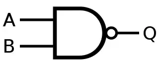
Here is the symbol for a NAND gate:
Logic gates can be combined to produce circuits that perform useful work. This circuit adds two bits; it's called a half-adder:

And this is a full adder:

Full-Adders can be combined to support multiple bits. This circuit is capable of adding two four-bit numbers:

With a bit of imagination, you can see how this could be extended to numbers of any arbitrary size, including a 32 bit or 64 bit addition operation.
Each operation so created with logic gates is mapped in the processor to a number called an opcode that the processor recognizes as the number corresponding to that operation. On an Intel processor, the opcode
5 id
maps to this assembly instruction:
add eax
Which is used in this assembly code:
    push    rbp
    mov     rbp, rsp
    mov     DWORD PTR [rbp-4], edi
    mov     eax, DWORD PTR [rbp-4]
    add     eax, eax
    pop     rbp
    ret
Which corresponds to this C code:
int twice(int num) {
    return num + num;
}
So as you can see, the instructions that you write in your software translate into machine instructions that map onto logic gates that are created from transistors that act as switching devices, precisely directing the flow of electrons to produce a specific result.
Disclaimer for the pedants: This is just an illustration. It is not meant to describe precisely what takes place in a given processor, but rather to illustrate the concept of mapping machine instructions to actual circuitry for educational purposes only. Don't drive or operate heavy machinery while reading this post.
Robert Harvey
- 198,589
- 55
- 464
- 673
-
-
1Hey, you're failing to confuse the newbie by using the less confusing convention that electrons flow in the direction of current rather then [the long established confusing convention](https://swahiliteknolojia.blogspot.com/2016/09/how-diode-works.html?m=1) that current is the positively charged flow of a lack of electrons. Next you'll be teaching people about [τ](https://tauday.com/tau-manifesto) and making them want to return their calculators. – candied_orange Nov 25 '19 at 03:51
-
@candied_orange, fundamentally the two conventions are equivalent. It's like asking whether the money in an accounting system is tracked by the debits or by the credits - the only real confusion arises when you try to characterise it as if only one of these things is occuring. Systematically, when I give you money, I also leave a hole in my wallet (or a quantity of negatively-charged money, that looks suspiciously like fresh air), and that's what an accounting system tracks. It's the same with electronics - it's fundamentally all about spatial exchange of charge, not one-way flows. – Steve Nov 25 '19 at 10:53
-
@Steve debit and credit are two different words. Current is just one with two meanings. One that makes sense now that we know electrons exist. The other that doesn't but is still followed in most all of the books. – candied_orange Nov 25 '19 at 14:16
-
@candied_orange, electrons exist, but so do electron-holes. It's entirely conventional to treat the electron as the "thing" and the moving part, and the hole as the absence of a thing. The holes are actually as measurable and quantifiable as the electrons (you can meter the current in a circuit based on the movement of the holes as easily as you meter the current based on the electrons), and every measurable electron has a corresponding measurable hole within the system, because the hole is an equally-and-opposite-charged counterpart to the electron, not a neutral absence-of-charge. – Steve Nov 26 '19 at 01:28
-
...as I say, the real confusion is that electronics tends not to be taught as an accounting system. The requirement of a *circuit* in which electron-holes have to be handled on an equal basis to the electrons and provided with a travel path, although a fundamental feature in practice, almost seems to be ignored in most treatments of the subject. – Steve Nov 26 '19 at 01:40
2
As noted in Robert Harvey answer, transistors are used to make logic gates. That does not cover how electrons move inside the transistors.
It is worth noting that logic gates, as any abstraction, can be implemented multiple ways. It is perfectly possible to make logic gates out of relays, or LEGO, or Dominoes or Minecraft Redstone, etc... and in theory you could build computers using those (except some like the Dominoes one would be single use).
For a whole computer, you will also want memory (which is possible to make out of transistors or logic gates, see Flip-flop) and a clock (which in modern computers will be based on a vibrating crystal. See the links on quartz watches and Piezoelectricity at the end).
Transistors do not rely on mechanical parts. That is, even though they act like a switch is not by moving things apart to disconnect them. I will skip Vacuum tubes (see How Vacuum Tubes Work if you are interested in that. Instead I will talk about transitors that rely on silicon semiconductors.
That is, silicon with impurities (doping) that result in a state with zero charge (the charges of the nucleus and the electron shell cancel), such that either:
- It has extra electrons (electrons that are not part of a bond). We say it is a N Type semiconductor.
- Are missing electrons (some bonds are not completed). We say it is a P type semiconductor.
I'll remind you that a bond is a hybrid orbital shared by multiple atoms, not that we need to understand that to understand transistors, but we do to actually answer "how electrons move".
Before we go into the transistor, let me talk about the diode. A diode has only one N type and one P type semiconductors. Naturally, electrons will flow from N type to P type, creating what is called a "depletion layer" where there are no longer electrons free to move.
In the depletion layer, the P Type took extra electrons and is now negatively charged. Similarly the N Type gave electrons and now positively charged.
The electrons jumping from orbital to orbital can emit light depending on the differnce of energy level of those orbitals. Which you would exploit if you wanted to make a Light Emitting Diode (LED), or was it a solar panel?
If we connect a power source such that it attracts electrons from the N Type, the N Type give even more electrons, widening the depletion layer. However, if we connect it such that it attracts electrons from the P Type, the P Type will give the extra electrons it acquired, allowing it to take more from the N Type. Allowing electricity to flow. For abstract, electricity will flow from N to P but not P to N.
You could push electricity the other way, and if the voltage is high enough, you would burn the diode.
Now, the transistor consist of three semiconductors. It can either be PNP or NPN. As you can imagine a PNP transistor will not allow electricity from any of the P ends. However, by adding electrons to the N in the middle, it can flow. Similarly, by attracting electrons from the P in the middle of the NPN it allows flow.
The middle section of the transistor is narrow and only requires a small current to overcome, however the transistor, once open can allow a bigger current to flow from a different source, acting as an amplifier (which is the other use of the transistor aside from making electronic switches).
By the way, make that too narrow and you have quantum tunneling causing problems. And the doubling the number of transistors per unit area thing breaks down.
About the representation of the transistor:
What we see here is a NPN BJE transitor. The arrow connector is known as Emitter, the one with the bar on the left is the Base, and the other one is the Collector. The base connects to the P section, while the others connect to opposite N sections. As I was explaining above, taking electrons from the middle section (the Base) will allow flow between the other connectors.
By the way, taking electrons means you connect the positive end of the power source.
Now, there are multiple ways to build logic gates out of transistors. I’ll take the same diagram Robert Harvey used:
The positive will be connected to the VCC (Voltage at the Common Collector) connector on top, and it tries to get electrons from ground at the bottom. However, those electrons can only flow if the transistors are open... that is, electrons can only connect ground to VCC if the possitive is connected to A and B. Otherwise, electrons will have to come from the A̅B̅ connector.
In other words, the A̅B̅ connector becomes a positive when the VCC is positive unless both A and B are positive. When both A and B are positive A̅B̅ is not positive. It is a NAND.
And yes, we represent it like this:

I will not talk about the adder, instead let us talk about memory. It will be an array of flip flops. Here is an example:

Flip flop made with NANDgates. Also known as S̅R̅ NAND latch.
This circuit has a feedback loop, it can take a while to understand. Perhaps an animation will suffice:

As you can see it has two outputs (Q and Q̅), and two inputs (S̅ and R̅). Those are inverted inputs. The idea of the inverted inputs is that you will keep them with voltage and interrupt them to signal them. If you signal the S̅, the output Q̅ will have voltage (and Q̅ will not), if you signal R̅, the output Q̅ will have voltage (and Q will not).
Q̅ is inverted Q.
That is a bit cumbersome to use. So we "gate" the flip flop:

Now, the value of the flip flop will only change if E has voltage. And the value set to Q will depend on either S or R having voltage... wait, we can do better:

Now, if E (enable) has voltage, Q will copy D, and Q will keep its value when E is disconnected. Yeah, memory!
*Q will keep its value when E is disconnected, as long as the memory has energy supply. Unless its state is affected, for example by cosmic rays (a type of soft error).
Alright, to make an array bank, we will have one of those flip flops per bit. We can connect the value we want to set to all of them (data bus), and only set E to the one we want to write (address bus). Except, you probably do not want to write a single bit. You want to set 8 bits, or 16 bits, or 32 bits, or 64 bits, or whatever amount of bits the CPU uses as base of operation.
Similarly, we can connect all the outputs Q of the memory to the CPU, and gate only what we want to read. In fact we can use the same buses, except we connect E and block Q to write and we connect Q and block E to read. I do not have the diagram to that.
Now, to execute code, CPU will be reading opcodes from memory. That is it will read from memory and do something depending on what it reads. Each CPU cycle (each clock cycle) the CPU will read the next opcode.
To do that, we keep in the CPU a memory (a register) that has the address in memory we want to access for execution and when the CPU takes a pulse from the clock, it will increment it to the address of the next opcode in memory.
How do you increment the register? Well you could it with adders, just add 1. However, it will probably be more efficient to chain flip flops. Which I'm not covering here. See the link on quartz watches.
Then it is a matter of using logic circuits to enable the part of the CPU that execute that particular opcode. For example, it could be doing operation with the internal registers of the CPU, or could be reading from memory to one of them, or writing one of them to memory.
As you can imagine the more instructions the CPU supports the more complex it becomes. And I haven't talked about cache, pipelines, multi-threading, etc...
Here are some links with more information from how computers work down to how electrons move:
- Crash Course Computer Science
- The Fetch-Execute Cycle: What's Your Computer Actually Doing?
- From NAND to Tetris
- Building an 8-bit breadboard computer!
- The Elements of Computing Systems: Building a Modern Computer From First Principles
- How a quartz watch works - its heart beats 32,768 times a second
- Piezoelectricity - why hitting crystals makes electricity
- Computerphile Logic Gates
- Karnaugh Maps & Logic Circuit Design!
- Logic Circuit Design using Boolean Algebra
- Making logic gates from transistors
- Crash Course Engineering (Semiconductors on Episode 22)
- Transistors - The Invention That Changed The World
- Transistors, How do they work ?
- How Does a Transistor Work?
- Crash Course Chemistry (Orbitals on Episode 25, The History of Atomic Chemistry on Episode 37).
- Hybridization Theory
- Crash Course Physics (Electric Charge on Episode 25, Quantum Mechanics on Episode 43).
- The history of atomic chemistry | Electronic structure of atoms | Chemistry | Khan Academy
- Modern Atomic Theory: De Broglie's, Schrodinger's & Heisenberg's Contributions
- Some light quantum mechanics (with minutephysics)
- Wave Function - Sixty Symbols
- Quantum Wave Functions: What's Actually Waving?
- Feynman's Infinite Quantum Paths | Space Time
- What is a Quantum Field?!? Behold. The foundation of the universe.
At the end the answer is that electrons are - in some sense - everywhere and take every path, even impossible paths. The answer to "How are electrons moved in processors/CPU?" is "Yes". However, that is not very useful.
Theraot
- 8,921
- 2
- 25
- 35