Questions tagged [creepage]

Creepage is the separation between two conductors as measured along the surface/layers of a board

For the most part creepage is the primary concern when it comes to "high voltage" and PCB design. It pertains to the safe distance between two conductor of differing electrical potential & the dielectric strength of the medium separating them.

For a given voltage, the distance that can safely & reliably support such a voltage is governed by

1) where in a PCB stack the traces are

2) what altitude the the card is at

For the most part the IPC2221A provides reasonable working rules for clearances.

enter image description here

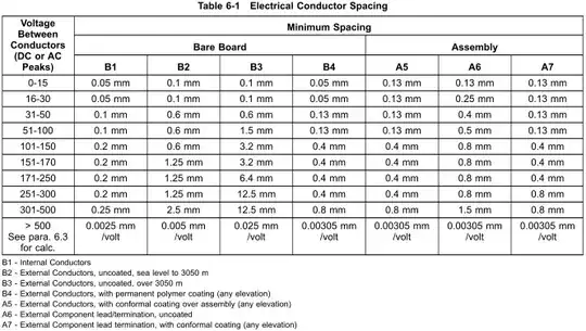
For voltages greater than 500V, the (per volt) table values must be added to the 500V values.

For example, the electrical spacing for a Type B1 board with 600V is calculated as: 600V - 500V = 100V 0.25 mm + (100V x 0.0025 mm) = 0.50 mm clearance

External traces require larger distances due to exposure to PCB contaminants that can reduce the overall creep distance.

50 questions
11
votes
1 answer

Clearance rules for outer/inner layers?

I found some information about general creepage and clearance distances here but it doesn't mention what is OK for inner layers, which are insulated and not subject to contamination the way outer layers are. Anyone know of a good reference for…
Jason S
  • 13,950
  • 3
  • 41
  • 68
9
votes
2 answers

What is a correct method to measure safe maximum voltage of a PCB?

I have a small (24 x 15 mm) PCB for a custom connector. It is intended for low voltage (< 48 VDC) applications, but I am interested in measuring it in order to provide customers a reasonable maximum voltage rating (de-rated of course). It is a 1.6…
JYelton
  • 32,302
  • 33
  • 134
  • 249
8
votes
2 answers

Will a cut or a slot in a PCB change clearance or creepage?

Does a cut or a slot in a printed circuit board increase clearance, creepage or both? Some say it will increase clearance, but I don't think clearance will change because, even with a cut in the PCB, distance over the air will be the same. Thus, a…
Bharav
  • 722
  • 2
  • 7
  • 21
6
votes
3 answers

Creepage for printed boards / printed wiring material and IEC 60664

In IEC 60664-1:2021 table F.5 (former F.4): Creepage distances to avoid failure due to tracking or 60950-1:2005 Table 2N – Minimum creepage distances the second and third columns are applicable for "printed boards" or "printed wiring materials". For…
Hellfish
  • 61
  • 2
6
votes
1 answer

Barrier and slot within reduced area on a PCB

Imagine this situation in a little area of your PCB: According to the worst case and used material, I need a creepage distance = 30mm. According some tables, clearance must be 30mm. First Red banana and black connector will have the same voltage:…
Suvi_Eu
  • 777
  • 6
  • 19
6
votes
2 answers

High Voltage Capacitor Lead Clearance

I am designing a high voltage board, 10,000 VDC. I wish to use a suitably rated capacitor such as the DHR4E4A102K2BB. When I have been studying the IPC-2221 and IEC 61010 standards the conductor clearance should be in the order of 0.00305 mm/volt,…
tomdertech
  • 193
  • 8
5
votes
3 answers

Why does increasing altitude (low air pressure) results in lower resistivity/ breakdown voltage?

I got this question because the creepage and clearance distances need to be adjusted for altitude. The higher the altitude, the higher the distances should be. It seems to me however that the contrary is true. What I mean is that we can tolerate…
HatimB
  • 826
  • 5
  • 15
5
votes
2 answers

High Voltage PCB

I am building a test probe PCB to test 75-115V. What is the minimum distance between traces that I should adhere to when building my PCB? I will have ground, 3v and 115V traces running next to each other, there will be low amperage, (1ma max), and…
Reid
  • 2,030
  • 1
  • 21
  • 38
5
votes
1 answer

Ethernet LED & Diffpair Clearance

How do you maintain creepage distance between diff pairs and the LED terminals on an Ethernet connector? My understanding is that based on EN60950, for 250V IT equipment, the air clearance is 2mm and the creepage distance is 2.5mm. Yet, the…
philby
  • 305
  • 4
  • 14
5
votes
1 answer

How does a fuse affect creepage reqirements?

I am designing a mains-powered device that has to comply with IEC 60079-15 (Non-incedive industrial eqipment). Creepage distances in this standard are inherited from IEC 60664, pollution degree 3. For \$230\,\mathrm{V}\$ AC it is \$4\,\mathrm{mm}\$…
venny
  • 3,058
  • 13
  • 16
4
votes
0 answers

IEC60950-1 - Does soldermask reduce creepage to pollution degree 1?

Since creepage distance requirements across a PCB are at least partially due to the potential of conductive pollution, is soldermask a sufficient coating to reduce fully covered traces to pollution degree 1 for determination of required…
A.Mac
  • 400
  • 1
  • 2
  • 8
3
votes
2 answers

What can I do about components with inadequate creepage?

I'm designing a device for use in a non-climate-controlled environment (garage, shed, etc.) If I understand it correctly, this puts me directly into pollution group 3 unless I can also engineer it to be inside a sealed enclosure, which is probably…
Matthew
  • 481
  • 2
  • 12
3
votes
1 answer

Creepage between layers on a PCB

I'm currently designing a power supply with high isolation between primary and secondary sides and have to comply to standard distances on clearance and creepage. My question is regarding creepage, I understand how it works on the same surface, and…
anzorein
  • 33
  • 2
3
votes
2 answers

Does recommended creepage distance apply to copper planes under soldermasks?

I have a design that requires around 0.5mm of creepage distance between conductors. TI said in this video that "creepage is the shortest distance between two uninsulated conductors along the surface of an insulating material". However, I've also…
Never
  • 31
  • 1
3
votes
5 answers

When to use slots instead of barriers in high voltage design?

I have read a lot of information about the clearance and creepage strategies, distances, materials, etc.. I am designing my first HV PCB, main LV circuit will be on TOP and HV (6KV) on the bottom. But I can' t avoid some low voltage points on the…
Suvi_Eu
  • 777
  • 6
  • 19
1
2 3 4