13

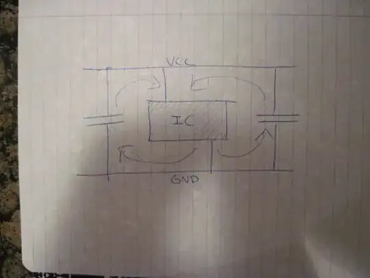
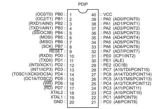
I'm making a board which will host an ATmega 162 microcontroller in PDIP package. Unfortunately, VCC and GND pins are diagonally arranged. From what I've read, the capacitors should be as close to the pins as possible for maximum effect.

enter image description here

Right now, I can see 3 ways to connect the capacitors. Run wires to the capacitors so that they are at equal distance from both pins, place capacitors near ground and run wire to VCC or place capacitors near VCC and run wire to ground. There's always the "none of the above" option too.

How do I make right decision in this case? Or is is irrelevant?

AndrejaKo
  • 23,261
  • 25
  • 110
  • 186
  • 1
    Breadboard or PCB? – Thomas O Feb 09 '11 at 01:07
  • @Thomas O Actually, I'll be using a prototyping board which has an individual solder pad for each pin and the pins are later manually connected together. I think that they're called Perfboard in English, but I'm not 100% sure. – AndrejaKo Feb 09 '11 at 07:53
  • 1
    Use a better package? The TQFP/MLF packages have more power inputs, plus with all the space you save you could fit all the decoupling caps you like. – Nick T Feb 10 '11 at 18:47
  • @Nick T Good suggestion (it's in Atmel's documentation as well), but I haven't advanced enough to be able to make my own PCB and to solder such packages. – AndrejaKo Feb 10 '11 at 20:56

5 Answers5

13

For these types of packages you should use at least two equal bypass capacitors, one at each side of the IC (one near ground and one near VCC). The parallel inductance of two traces to two different caps lowers the total trace inductance and the current flowing from each bypass cap in opposite directions helps cancel out EMI. See Henry Ott's book "Electromagnetic Compatibility Engineering" for more details here. Apparently this technique reduces noise by a significant amount and will also help functionally. This technique taken to the extreme would involve using a power and ground plane and surrounding the entire chip with bypass capacitors, or if you have the money to spare, using buried capacitance planes, but simply using two caps at either side of the package makes a large and measurable difference (as opposed to just at the VCC side) (I'm too lazy to look it up but I think we're talking 10dB+ improvement).

enter image description here

EDIT: Added my cheesy drawing. The arrows are supposed to show the canceling current loops (one clockwise the other counterclockwise), but note the capacitors should be placed closer to the chip then I drew.

bt2
  • 3,784
  • 2
  • 25
  • 28
  • I didn't know this - thanks! What is [the book](http://www.amazon.com/Electromagnetic-Compatibility-Engineering-Henry-Ott/dp/0470189304) like? – tyblu Feb 09 '11 at 03:27
  • 1
    I attended a Henry Ott seminar and it blew my mind. There are a lot of conventional practices out there today that may be ineffective or even make things worse that he covers with down to earth explanations and studies or data to back it up. If you can't get work to send you to one of his seminars (or even if you can) I'd highly recommend the book. It's my EMC bible. It may be my favorite engineering book of all time. It covers almost everything and is written in a very understandable manner. It's also packed with great sources for further reading on almost every subject. – bt2 Feb 09 '11 at 03:35
  • Can you provide a sketch of the capacitor arrangement? – AndrejaKo Feb 09 '11 at 11:56
10

enter image description here

markrages
  • 19,905
  • 7
  • 59
  • 96
7

The decoupling capacitor goes as close to the power pin as possible, as the power line has a higher impedance than the ground reference. There should be a large ground plane, ready to provide a very low impedance path. A power plane is sometimes employed in multilayer (4+) designs for, among other things, a low impedance source.

You talk about wires, which leads me to believe you are using a breadboard. In this case, decoupling capacitors are just as important, but parasitic inductance and capacitance and ohmic contacts will mask their effects. Use the power rails for power and ground, and tie them together in multiple locations -- no ground loops! I wouldn't bother with anything other than a large electrolytic (10uF) in a breadboard unless it doesn't work, as it is only for prototyping simple circuits. (Does this work?) Troubleshooting decoupling requires the real layout (if the final product is in a breadboard, then go for it).

tyblu
  • 8,167
  • 6
  • 40
  • 70
  • He said in a comment that he was using perfboard. – Kevin Vermeer Feb 09 '11 at 14:33
  • I'm using a breadboard and I'm trying to figure out exactly what's going on with a decoupling capacitor ... what exactly does *Use the power rails for power and ground, and tie them together in multiple locations -- no ground loops!* mean? If I connect ground rail to power rail with a capacitor, is that not a loop (as ground rail is connected to GND and power rail is +5V)? I was just going to literally drop a capacitor in between VCC and GND on each of my shift registers but now I'm confused... Can you possibly provide a picture/diagram? – redstarcoder Jan 19 '17 at 17:20
  • [This image answered my comment question.](http://i.stack.imgur.com/rRCDN.png) – redstarcoder Jan 19 '17 at 17:33
  • Outstanding diagram explaining the key parameters, and also excusing @markrages's answer, but a major problem seems to be wire lengths when using a breadboard. Is everyone here agreed this is the best possible solution, lead lengths notwithstanding, when using TTL chips on a breadboard? Understood, decouplers around the circuit are also essential. Is the solution in the diagram preferable to two identical caps from the power and ground pins to the nearest power and ground rail (i.e.on different sides of the board) or does this violate the principle, despite saving greatly on line length? – Hektor Jun 26 '23 at 16:21
5

For a PCB design, I almost always use a ground plane and for chips with opposite power pins I place a cap next to the power pin and ground the other end. The ground plane has a low inductance which reduces the effect compared to wiring a single trace to Vss. The goal of the decoupling cap is to provide a local current source for the chip, so this works well.

If it's a breadboard, I usually just solder some wires to a 100n cap and wire it over the chip. Messy, but it works.

Thomas O
  • 31,546
  • 57
  • 182
  • 320
  • .. short version of what I wrote, and earlier! +1 for getting to the point! – tyblu Feb 09 '11 at 01:11
  • Well, is this a good approach in case of EMI? [According to Olin](http://electronics.stackexchange.com/a/15143/5035), it is not :) Damn, PCB layout is a pain in the ass! – abdullah kahraman Apr 06 '12 at 07:05
0

Overall distance matters, as inductance increases as you increase the wire distance. However, the position of the capacitor along this wire should not matter.

cksa361
  • 3,814
  • 7
  • 33
  • 49