8

enter image description here

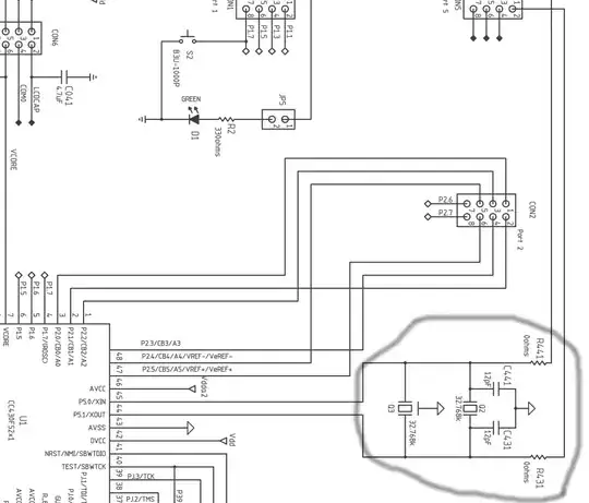
why there are two crystal oscillators connected in parallel in the circuit above? i am familiar with the configuration of Q2( look at the schematic) but what is the purpose of Q3? do i really need to implement it? if yes, why?

the chip is CC430F5133. datasheet

Maxwell S.
  • 183
  • 1
  • 3
  • 2
    One or the other is a "Do Not Place" or "Do Not Stuff". That information might be in the BOM for where ever you got that schematic, because it wasn't from the datasheet. The zero ohm resistors are another clue to that. – Samuel Jan 07 '14 at 19:46
  • Are you using this in wireless application? Have you try to operate without any crystal connectet or other frequency like 27MHz? – GR Tech Jan 07 '14 at 20:39
  • @GRTech There is a separate crystal that is used for the wireless aspect of the chip. – Kellenjb Jun 10 '14 at 01:10

3 Answers3

11

If I drew a circuit with two crystals connected in parallel it's because on the Bill of Material I would be choosing either one or the other. The PCB layout would be tracked to take version A or version B but only one would be soldered to the PCB. This gives me the ability to buy version B if version A became unavailable.

It's like showing pull-ups and pull-downs on the same IO line - it makes no sense to fit both but, as a design, I may want the option of fitting one or the other.

Andy aka
  • 434,556
  • 28
  • 351
  • 777
7

Those are crystals or ceramic resonators, not oscillators.

Q2 is a "bare" crystal, and needs the added capacitors to operate correctly.

Q3 appears to have the necessary capacitors internally.

The assembly instructions for the board will say to either install Q3, or install Q2, C441, and C431.

Peter Bennett
  • 57,014
  • 1
  • 48
  • 127
-1

It is a mistake as shown.
Only one is used. I'm not sure why the osc leads are brought off to a header like that either, poor design for several reasons.
Go back to app note and use that.

  • 2
    No, I don't think it is an error. The two pins that the crystal(s) are connected to can also be used as GPIO, if the chip is configured to use an internal clock source. The two resistors R431 and R441 would be installed if the pins were used as GPIO, and removed if either crystal configuration was used. – Peter Bennett Jan 08 '14 at 01:45
  • This is not a mistake. The PCB has 2 different footprints with 2 different designators. Schematic reflects that. Although, yes, only one of the footprints is populated in the PCBA. – Nick Alexeev Jan 08 '14 at 01:45
  • the osc are two different parts, perhaps they had a parts supply problem, anyhow they still could have combined it into one place on the layout for space reasons, and show one part on the schematic, call out which one by the PL – Gammara Smith Jan 08 '14 at 02:52
  • No, they couldn't have. Those are two different parts. – Ignacio Vazquez-Abrams Jan 08 '14 at 05:07