3

I am trying to learn electronics by looking at simple circuits and see how engineers get the job done.

Looking at a PCB featuring only one Texas Instruments ADS1115 ADC, I see that:

  1. They bridge VCC and GND with a capacitor as close as possible to the power lines arriving at the PCB. I guess it's 100µF (shown in the picture).
  2. They do the same on the VCC and GND as close as possible to the chip (not shown in the picture).
  3. They have pull-up 10K resistors on the SDA, SCL and ADDRESS lines. I guess it's because they wish those to be high when not driven (not shown in the picture).

However, I do not understand why they have two parts (black 0805) inserted in the VCC and GND lines arriving on the board (shown at the top of the picture). Are these resistors ? What would their purpose be ? The board can be powered from 1.8 to 5 V.

enter image description here

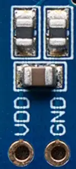
Maybe they are only diodes? In that case, the polarity should be marked. And there would be a voltage drop across.

I am also puzzled, because these parts are across the VCC as well as the GND. In my mind, there is never any part splitting the GND line.

PeterG
  • 89
  • 1
  • 9

3 Answers3

5

I think they may be inductors - a series inductor and a parallel capacitor across the target chip's power and ground line offer greater power supply rejection (in a lot of cases) compared to just a capacitor and no series component. Care has to be taken though; the series L and parallel capacitor can form a resonant tuned circuit and exaggerate certain frequencies of noise coming from the digital supplies.

Given that this is an TI chip, there may be a kit you can buy from them that uses this part - try looking up the details of the kit to see if you can track down whether these parts are inductors or not.

Andy aka
  • 434,556
  • 28
  • 351
  • 777
4

"I am trying to learn electronics by looking at simple circuits and see how engineers get the job done." Bad idea unless you know for sure it's a good design. There is a lot of crap published out there. In fact, bad designs are more likely to be published than good ones. Professionals that create good designs are usually too busy to write up a web page, don't think their design is a big enough deal to bother writing up, and often can't disclose their schematics anyway due to confidentiality issues. It's the hobbyist who can barely spell "EE" and just spent a week getting a arduino to blink a LED that will proudly publish the results of his herculian effort for all to see.

  1. I don't see any picture of a 100 µF capacitor. You also have't shown the schematic, so I can only answer in general. It is usually a good idea to put a reasonable energy storage cap, like 100 µF, at the power supply input of a board. This is so that you can tolerate some impedance in the power supply feed. The local capacitor will supply medium-time current surges required by the board before the current can build up in the possibly long wire back to the power supply. The power supply may also take some time to react.
  2. This is called a bypass cap. It's the same concept but even more local and for higher frequencies. I go into more detail here.
  3. IIC bus lines are specified to float high and be actively pulled low. The 10 kΩ pullups provide the floating high part. Basic IIC is limited to 3 mA source current when held low. Note that when pulled up to 5 V, a 10 kΩ only provides 500 µA. That's OK, but the pullup therefore could be lower, which would allow the bus to run at higher speed.
Olin Lathrop
  • 310,974
  • 36
  • 428
  • 915
  • So scathing of hobbyists Olin! :) Professionals should publish their designs where they can, so everyone can learn. Better yet, they should come to EE.SE and share their knowledge. ;) – geometrikal Jan 04 '14 at 22:58
2

These are MMZ2012Y152B ferrite filters and your 3rd guess about I2C pullups is correct.

The schema including components names is on the manufacturer Github.

user35082
  • 68
  • 1
  • 5
  • `your 3rd guess is correct` Is that referring to what the OP said about SDA, SCL lines? – alexan_e Jan 04 '14 at 14:50
  • Yes, a great link about it is : [Effects of Varying I2C Pull-Up Resistors](http://www.dsscircuits.com/articles/effects-of-varying-i2c-pull-up-resistors.html). – user35082 Jan 04 '14 at 14:52
  • The thing is that pulling these lines high isn't really a matter of the designers wish but rather a requirement for I2C lines. Your link was mis-formated but I'm sure you meant [this one](http://www.dsscircuits.com/articles/effects-of-varying-i2c-pull-up-resistors.html) – alexan_e Jan 04 '14 at 14:59
  • Thank you for your reply. That's it, indeed. Here is the link we all try to post : http://www.dsscircuits.com/index.php/articles/47-effects-of-varying-i2c-pull-up-resistors – PeterG Feb 22 '14 at 21:03