I recently found "ZofzPCB" (https://www.zofzpcb.com/). It seems to do a fairly stellar job of making a PCB look absolutely beautiful and geometrically accurate.
I've been using it at work to sanity-check Gerber files (it's natively supported format) before manufacture.
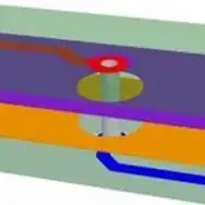
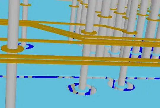
In particular it does a good job of showing layer connectivity for vias, and PTH features. Thermal reliefs of all kinds are nicely displayed.
One of my favourite features is the "Spread" layers view, where it explodes the PCB and elongates all the vias to reveal all net / layer / plane connections.
FD: (I'm not affiliated in any way with ZofsPCB software)