4

Edit/added - RM: See Karl's prior question of December 20th last DS1822 1-Wire Sensor, Parasitic Power, and Strong Pull-Up Circuit which gives a very clear explanation of what he is actually trying to achieve. The following material is related to his attempt to understand the high side strong-pullup requirement of the IC concerned. < /edit >


I have been looking through many of the posts with MOSFET in them, but can't seem to find exactly what I'm looking for. Apologies in advance if this is a common or duplicated question.

I have obtained an N-Channel MOSFET (IRLB8721PBF-ND) (http://www.irf.com/product-info/datasheets/data/irlb8721pbf.pdf) to use as a logic level MOSFET.

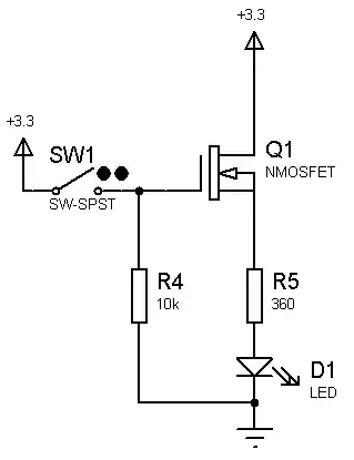
To test out the behavior I'm expecting to see with a 3.3v MCU, I hooked the Gate to a 3.3V power source with a 10k ohm pull down resistor. Drain was hooked to the same 3.3V power rail and Source connected to a 360 ohm resistor running through an LED to ground.

The behavior I saw regarding voltage was not what I expected. It seems that the voltage measured at the Drain is 3.3V (expected) and at the Source is 1.65V (not expected).

Disconnecting the LED and current limiting resistor brings the Source to 1.93V.

What I am attempting to determine is if the 1V+ voltage drop I'm seeing is due to the MOSFET's diode forward voltage maximum of 1V, or if there is something else at play here.

The intention of using the MOSFET is ultimately use it to directly connect a parasitic 1-wire device to the power rail during current intensive operations to retain the needed ~2.8V level.

This shows me that the setup I have now would not work. If my assumption is correct, do 'logic level' MOSFETs exist that have an almost negligible forward voltage drop?

If my assumption is incorrect, then perhaps I've wired something incorrectly and this setup could still work.

Additionally, I've seen recommendations to place a current limiting resistor between the MOSFET Gate and an MCU pin to avoid high current levels that may come back through. With the already existing 10k pull-down resistor from the gate, would this not create a voltage divider? I believe that's the behavior I saw at one point earlier in my experimenting.

edit
This schematic shows a modified circuit based on the request to move the LED and resistor to Vcc and the drain. Originally, they were both located between the Drain and ground. I guess at this point I have some confusion over high side / low side and why this now works. My actual intent for the circuit is to use the same schematic but instead of an LED/Resistor, the MOSFET will be used to provide increased voltage for an open drain port on an MCU connected to a 1-Wire parasitic device.
enter image description here

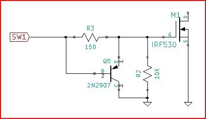
Here's the schematic I'm ultimately aiming for with the MOSFET. It comes from from Maxim's own datasheets.
enter image description here

paul_25
  • 55
  • 1
  • 1
  • 9
  • Karl, a schematic of your experiment setup would make the question a lot clearer. You can link a picture, and someone with enough rep will inline it. Or, you can use CircuitLab. Judging from the description, however, it looks like you're trying to use an N-ch MOSFET as a high side switch, and not driving the gate high enough. – Nick Alexeev Jan 02 '14 at 23:25
  • 1
    This looks like the common high side/low side error. Use a P channel device, or move your LED and resistor to Vcc and the drain, and ground the source. What does that do? – C. Towne Springer Jan 02 '14 at 23:26
  • I have uploaded a schematic at: https://dl.dropboxusercontent.com/u/35207477/mosfet.png which shows a modified circuit based on the request to move the LED and resistor to Vcc and the drain. Originally, they were both located between the Drain and ground. I guess at this point I have some confusion over high side / low side and why this now works. My actual intent for the circuit is to use the same schematic but instead of an LED/Resistor, the MOSFET will be used to provide increased voltage for an open drain port on an MCU connected to a 1-Wire parasitic device. – paul_25 Jan 03 '14 at 00:38
  • The schematic I'm ultimately aiming for with the MOSFET can be seen here as well: https://db.tt/wI01RNQF (This is from maxim's own datasheets). – paul_25 Jan 03 '14 at 00:47
  • @Karl_34: That schematic needs a P MOSFET. – Laszlo Valko Jan 03 '14 at 01:33
  • As indicated by the inversion circle at the gate. – Ignacio Vazquez-Abrams Jan 03 '14 at 01:34
  • Thank you all for the comments. The high side / low side comments gave me some key points to research further and I understand that given the high side switching I'm attempting to do, the P MOSFET is appropriate. I am hoping that I can locate something appropriate to work with the 3.3v MCU and 3.3v power source. – paul_25 Jan 03 '14 at 04:49
  • The [Vishay SUB75P05-08](http://www.vishay.com/docs/70891/70891.pdf) MOSFET that you asked about below is massively massive overkill for this task AND will only just work in some cases. The Vthgs is shown as 1/2/3 V min / typical/max at Ids = 250 uA. If you are unlucky enough to get a worst case one (unlikely but possible) with Vthgs = 3V (or -3V actually) then 3.3V of drive will "only just" be enough drive to turn it on at the few mA level. While in most cases you would be able to source many Amps from the same part with 3V3 driver, there are smaller, cheaper, better parts for the task. – Russell McMahon Jan 03 '14 at 07:13
  • FYI - despite my prior comments on asking the right question (which are of course valid) you presentation, quality of general question asking and approach and description of what you have tried and why ... , are generally in the extremely good, excellent and awesomely-acceptable area. Keep that up and you can expect to learn much about electronics and have an enjoyable journey to boot. – Russell McMahon Jan 03 '14 at 07:23
  • Aha. Enlightenment. | I've just looked at your question of December 20th, which I had not seen until just now - [DS1822 1-Wire Sensor, Parasitic Power, and Strong Pull-Up Circuit](http://electronics.stackexchange.com/questions/94204/ds1822-1-wire-sensor-parasitic-power-and-strong-pull-up-circuit). ... This gives a very clear presentation of your requirement. A reference to this prior question (which as far as I can see you didn't) would probably have led to a much better result. (But many people in future would have missed out on the useful material posted by others :-). ) – Russell McMahon Jan 03 '14 at 07:26

3 Answers3

5

You have received a large amount of useful input related to the question that you asked and it will be of assistance to others who read these answers in future.

However, you have been wasting people's time and confusing your self because you stated what you thought you needed to do to fix your problem instead of telling your people what your problem is. While there is some overlap the answers that have been given mainly relate to things that you are not trying to do. While they do somewhat address what you are trying to do, the diagram that you provided would make almost no sense in most contexts and is NOT doing what it appears to be doing.

Lesson: "Tell us what you actually are trying to do and we will tell you the best way to do it".

Real question: See Maxim DS1822 Data Sheet -
PAGE 5 - POWERING THE DS1822 and
page 6 SUPPLYING THE PARASITE-POWERED DS1822 DURING TEMPERATURE

In the related diagram below Vpu is a "weak pullup" and the FET is a "strong pullup".
When the Vdd pin is grounded, power supply energy may be provided via the DQ line and is stored in an internal capacitor Cpp (C parasitic power). During most portions of operation the "parasitic" feed provides enough current Ipp at an acceptable voltage to power the IC. During some operation Ipp is inadequate and the iC must either be powered via Vdd or via a higher current source (see data sheet page 5). During these high current operations the FET is turned on to provide extra supply current. This low resistance power feed clamps the bus high and presents it being used for signalling by other ICs on the bus, so the 'strong pullup' is enabled only for as long a period as required.

enter image description here

SO:

You do need a FET for pullup, you do need a high side FET, this need is most simply met with a P channel FET - all as advised by others.

As Vmicrocontroller (Vmcu) is >= V1_wire_bus, the FET is not being used as a level converter but as a high side power supply switch.

Choosing a MOSFET:

Connecting a suitable P Channel MOSFET as shown in the diagram will fill the need. Many FETs will do the job.

Rdson / On resistance: MOSFET must have low enough on resistance = Rdson for the task.
A MOSFET that dropped 0.1V at 2 mA would probably suffice
Rdson = Vdrop / Iload =
= 0.1v/2 mA = 50 Ohms.
You'd have immense difficulty buying a P Channel FET with Rds = 50 Ohms = normally available ones are typically 50 to 5000 times BETTER (lower Rdson) ie 1 Ohm down to say 10 milliOhms.ie ANY P Channel MOSFET that meets other specs will have an OK Rdson

Gate operating voltage = Vth or Vgsth:
Vth or Vgsth should be << Vcpu.
ie the μP (microprocessor) should easily drive the MOSFET.
A 3.3V μP will JUST operate a MOSFET where Vth = 3V.
Operation will be better at Vgsth = 2.5V
and better again at 2V. Lower again does not hurt.

Vds_max > say 10V is OK - 20V or 30V better. > 30V OK.
Ids_max is so low as to be met by anything.

The horrible BSS184 - datasheet here is 20 cents in 1's at Digikey and does the job well enough. Digikey and others have many more that will do a better job - but not needed here.

SmokinGrunts
  • 138
  • 1
  • 8
Russell McMahon
  • 147,325
  • 18
  • 210
  • 386
  • Thank you. Although I had a target circuit in mind from the data sheet, I was also misunderstanding the MOSFET in general. Your answer is precise and exact and I will follow your advice for future posts. – paul_25 Jan 03 '14 at 06:17
3

In order to saturate a high-side NMOSFET driver you need to elevate the gate to at least VGS(th) above the desired source voltage. Since the typical value for that part is 1.8V, you can only get a maximum of 3.3V - 1.8V = 1.5V or so at the source. Consider switching to a PMOSFET so that the math works out properly for your situation.

Ignacio Vazquez-Abrams
  • 48,282
  • 4
  • 73
  • 102
  • I'm confused here as the part is described as being able to be driven by anything from as low as 2.8v up to 5v due to the low threshold voltage. This came from the description from adafruit.com. – paul_25 Jan 03 '14 at 00:55
  • @Karl_34: That is correct. But those are referenced to the source. With low-side driving, the source is at ground. With high-side driving, the source is at the target voltage for the load. – Ignacio Vazquez-Abrams Jan 03 '14 at 01:07
1

The mosfet is controlled by a voltage applied between the gate and source pins.
For a N-mosfet the gate should be more positive than the gate.

Now lets examine what you are trying to do.

enter image description here

When the gate is grounded the mosget is off so there is no current through R5 and the source is at 0v.
When you apply 3.3v to the gate then you apply a Vgs of 3.3v BUT as soon as the mosfet starts to conduct the voltage at the source rises (becomes more positive) and as it rises Vgs gets lower and lower (since Vgs is referenced to the source and not the ground) until the mosfet reaches a balance. That balance point is related to the Vgs-th (so will be different for each mosfet) and will keep the mosfet in a half open state.
There are two forces that keep this balance, if the mosfet tries to conduct more then the source will become more positive and Vgs will decrease, if on the other hand it tries to conduct less then Vgs will increase.

To avoid this problem with a N-mosfet as a high side switch you must either use an isolated power supply that will be applied between source and gate and will add over the existing voltage or a higher voltage from the one that is connected to the drain (if not available it can be generated with a bootstrap circuit).

In your particular case the best solution is to simply use a Pmosfet as Ignacio Vazquez-Abrams has suggested.

Regarding the gate resistor, it is not really necessary for static operation (unlike fast PWM). The mosfet behaves like a capacitor, it needs to be charged in order to turn on and to discharge in order to turn off. As soon as it does turn on (or off) it doesn't draw any current. The capacitance is about 1nF according to the datasheet.

alexan_e
  • 11,070
  • 1
  • 28
  • 62
  • Thank you for the detailed description. Moving to a P MOSFET, can you comment on whether a part such as this: http://www.vishay.com/docs/70891/70891.pdf would be appropriate given the gate would be driven by a pin on a 3.3V MCU and the source connected to a common 3.3V power source? – paul_25 Jan 03 '14 at 05:37
  • @Karl_34 Vgs-th is specified as -3v max (note that this specification is for just 250uA current) so 3.3v is too close to that, you need a mosfet with has an even lower Vgs-th – alexan_e Jan 03 '14 at 08:27