6

How can we estimate maximum switching frequency of GPIO FPGA pins? What is maximum data rate achievable when connecting two FPGAs together without using of integrated high-speed transceivers? Or when we are bitbanging GPIO to VGA, what is maximum pixel clock?

I'm interested in modern cheap Altera devices, like Cyclone IV, Cyclone V (E version, not GT), and Xilinx devices like Spartan 6.

There are some figures in datasheets saying 300-400 MHz for GPIO pins, but are they real? How can we drive pin at 300-400 MHz when maximum core clock is only 100-150 MHz?

osgx
  • 665
  • 1
  • 10
  • 19
  • Many FPGAs have PLL/Clock blocks that can multiply an input clock up to your desired frequency. – dext0rb Jan 01 '14 at 23:10
  • dextorb, yes, but I think I can't have logic clocked higher than 150 MHz in my Cyclone IV (C6 speed grade). – osgx Jan 01 '14 at 23:45
  • 1
    I think that's the max REFCLK, not the maximum logic speed, which is determined by propagation delay and flop setup/hold times. If it says 400MHz in the datasheet I would expect to be able to achieve that. – pjc50 Jan 02 '14 at 01:07
  • I don't get why people often want FPGA for what they are not designed to. A low-end FPGA like the Cyclone series are cheap but not designed to run high frequency core clock, if you want your design to run at a high frequency you need to take a higher end FPGA. Its like a processor : an Atom and a Core i7 don't cost the same but also don't have the same performances too. Keep also in mind that with a FPGA you can do concurrent actions whereas with a MCU your are working step by step (simplifying). So even if you're clock is low you can manage to optimize your design ;) – zeqL Jan 03 '14 at 08:58

3 Answers3

7

Short answer: yes, you can achieve 400MHz IO on the general user IO on the Cyclone V depending on your speed grade. For example the hard memory controller can run at a 400MHz. Note also that the fastest speed-grade parts can support an internal global clock of 550MHz. I'm not sure where your 100-150MHz value comes from but that's not a device limitation ;) In practice the top-end of the device capabilities will be very difficult to achieve but you should be able to get close.

If you are trying to maximise bandwidth between FPGAs the number of IOs will be limited by your package choice, however there are a number of other factors to consider when estimating bandwidth:

  1. Layout and signal integrity. To achieve the memory interface speeds you need to have well matched, relatively short traces. If you are unable to match the traces and keep them short then you may experience signal integrity issues that reduce the frequency below what the device can actually support. If you must use long traces you might consider sacrificing IOs for integrity by using LVDS rather than SSTL or similar.

  2. Bus skew. If you're trying to maximise bandwidth by bundling lots of IO onto a wide parallel bus you may have difficulty keeping all the bits synchronous and without some form of calibration this will drastically reduce the frequency. External memory interface have a calibration phase that dynamically adjusts the delay on each bit of the data bus to compensate for skew between bits, you will likely need to do something similar. For example on Cyclone V you can adjust the output delay from 0 to 150ps in 50ps increments but be aware that these values aren't always changeable at run-time so check the datasheet carefully.

  3. Clocking. You'll almost certainly want to use a source synchronous clocking architecture rather than sharing an external clock. This will affect your choice of pins.

Another gotcha when using wide interfaces is the mismatch in internal routing delays to get to the pins - even if your traces are perfectly length matched the internal delays may skew the bus more than you can compensate for on the receiver so always run your design through the tools and feed this information into your board design. Sometimes it's better to have deliberately mismatched PCB trace lengths to compensate for delays in the device!

Chiggs
  • 670
  • 4
  • 5
3

Source synchronous outputs from GPIO can go much faster than the internal logic of the FPGA. As FarhadA stated this is due to all of the high speed IO interfacing requirements even low end FPGAs have to meet today (DDR2/3/4 memory, cameralink, mipi, high speed ADCs, etc).

For example the Spartan 6 can do up to 1050Mb/s http://www.xilinx.com/support/documentation/application_notes/xapp1064.pdf See also page 18 of the Spartan 6 datasheet http://www.xilinx.com/support/documentation/data_sheets/ds162.pdf

To achieve these rates the outputs are serialized and internal processing is done at a slower wider signal. Specifically the ISERDES and OSERDES blocks are hard ip blocks in the IO tiles of the Spartan 6 FPGA. Xapp1064 will reference much of the appropriate documentation.

davidd
  • 513
  • 2
  • 5
2

The speed of the GPIO can be 2-4 times the speed grade of the FPGA itself. The IO blocks of the FPGA, are designed to support higher speed than the FPGA can support. This is because many of these IOs are created to support high speed IOs such as PCIe, USB 3 or even 3 and RapidIO just to mention a few.

Even if your FPGA's maximum clock is 400MHz, you can access IOs at twice that speed using the DDR blocks of the IO or even 4 times that using a QDR block.

It is also possible to serialize and de-serialize the data to/from the IOs, which makes it possible for a low cost FPGA to access high speed interfaces.

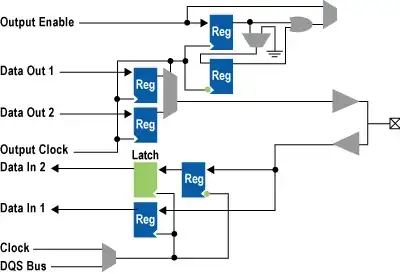
For example Altera Stratix II has the following IO blocks: enter image description here

I am sure you can find similar description from other FPGA companies as well.

You can take a look at this PDF file from xilinx regarding high speed serial IO capabilities of their FPGAs.

http://www.xilinx.com/publications/archives/books/serialio.pdf

For example, in my last project, we managed to connect and FPGA to PCIe Gen 3 at 8Gb/s even thought the maximum achievable internal speed for the FPGA was about 250MHz. In that project, we used a special PCM module, you can read more about PCIe access support of Xilinx FPGAs at: http://www.xilinx.com/technology/protocols/pciexpress.htm

FarhadA
  • 1,379
  • 1
  • 10
  • 20
  • 1
    But as I know, PCIe and other high-speed interfaces are implemented with hardware transievers, not with usual GPIO. As GPIO I mean the pins without hardware highspeed parts. – osgx Jan 03 '14 at 08:52
  • 2
    OP says without using the integrated high speed transceivers so the mention of PCIe gen 3 and USB 3 is misleading as these protocols are not possible using GPIO. – Chiggs Jan 07 '14 at 23:29