Hi I try to connect 2 devices. The first one sends a pulse to the second. The second has a 3.3 V input. And the output pin from the first device has a voltage of around 7.3V. VCC of the first is 12 V.
Information from the first device: the pin is active low. What does it mean?
I thought a voltage divider was a good idea to transform the 7.3V to 3.3V. (R1 =2k2 and R2=1k8)
But when I connect the output pin of the device 1 to R1 and his gnd to the gnd of the voltage divider, the 7.3 voltage drops and the voltate between R1 and R2 is 0.3V. Why does the voltage drop more than expected? is there a solution?
Asked
Active
Viewed 1,415 times
0
user34835
- 1
- 1
-
2What type/kind are the two devices? What is the current level that the receiving device requires in the input (input impedance)? – alexan_e Dec 29 '13 at 20:06
-
What is the output impedance of device 1? – Andy aka Dec 29 '13 at 20:33
-
The first device is a coin acceptor and the second device is a 3.3V device (microcontroller board). About the impedance, I have not that information: only the voltage. I cant know what is the input current. But I don't understand why the voltage drops without connection to the second device. Only with the voltage divider the voltage drops in a way I dont understand. The voltage would drop to 3.3V but I measure less than 1 V. – user34835 Dec 29 '13 at 22:01
-
I think the maximum output current from device 1 is 100mA – user34835 Dec 29 '13 at 22:34
1 Answers
2
Active low means that the function of that pin is enabled when the signal on it drops to 0V of below the Vi(l) level specified in the data sheet. For instance, if a chip as a #EN or nEN line, this means that the device will be enabled when the signal on the #EN or nEN line drops low.
As for the voltage drop, you need to examine the data sheet for the pin impedance and whether it is classifies as Open collector/Drain. Without knowing which devices you are using, it is difficult to comment further. If the input side of your second device has some impedance, then it will appear in parrallel with R2. A better way to achieve level convertion is to use a level shifter or a simple low VGs fet arrangement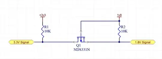
Any FET may be used provided it satisfies the shift voltage and VGS(on) requirements.
Martin
- 866
- 6
- 7
-
thanks ... what is the function of R1 and R2 in the schema? Maybe is that what I need ? I mean maybe I need to put a R1 beside the output signal (pulse) – user34835 Dec 29 '13 at 22:15
-
The function of the Resistors is to pull up the signal lines when they are relaxed. Oterwise they may float to an unknown state and cause false triggering of your inputs. R1 is particularly important because the FET operates in Open drain configuration. Without a pullup (R1), the Drain of Q1 will float giving a random state on the 3.3V signal label. Simialrly with R2. R2 stops the FET from conducting by lifting the source pin to 1.8V. This keeps the FET off. – Martin Jan 01 '14 at 21:18
-
The ["Using the Logic Level Converter" tutorial](https://learn.sparkfun.com/tutorials/using-the-logic-level-converter/resources--going-further) has some links to documents that go into much more detail about the function of R1 and R2 pull-up resistors. – davidcary Jan 02 '14 at 00:35
-
related: [bidirectional 5v-3.3v level shifter](http://electronics.stackexchange.com/questions/97889/is-there-any-bidirectional-5v-3-3v-level-shifter). – davidcary Jan 28 '14 at 13:14