9

I have a very good op amp (AD8551) that I use to dynamically amplify a very small signal (2x, 10x, 100x, 1000x gain).

The problem is that there is a noticeable noise level at 100x and 1000x gain, and it has a weird constant shape.

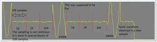
If I power the circuit with a poorly stabilized power supply and connect the input of the amplifier at GND, I get a large noise level at 1000x as seen in the picture bellow.

If I power the circuit with a better stabilized power supply, the noise is still present at 1000x with the same waveform, but lower amplitude. And no matter what power supply I use the weirdly shaped noise doesn't disappear.

Since my AD8551 has a PSSR of 130 dB, I thought that TL431 used for biasing the input may be at fault. So I left the poorly stabilized power supply for the op amp and used the better one for the TL431, but the output is the same. Stabilizing the voltage on the resistor in the cathode of TL431, doesn't change anything.

amplifier schematic

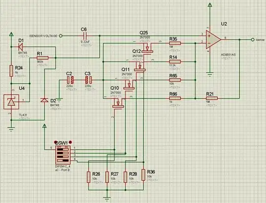
The image below is an output sampled by a microcontroller with it's internal ADC. As you can see at 1000x the output swings almost full range. The reason 100x is missing in this test is because I replaced the 1MΩ R21 with a 100KΩ resistor and 1KΩ R66 with a 100Ω one, resulting in 1.1X, 2X 10X and 1000X amplification. I did this because I was fearing that the feedback resistor R21 might be too big to bias the op amp negative input, even though AD8551's input bias current is rated max 2nA. The change did slightly diminish the amplitude of the noise. enter image description here

Does the Vcc have to be dead quiet even though the op amp's PSRR is 130 dB? Is it the input bias causing this problems?

I can't figure it out, especially since I don't have access to an oscilloscope. All I have are the readings from the microcontroller saved on a SD card.

Chris
  • 554
  • 6
  • 13
  • This looks a lot to me like there is a bad connection somewhere. I am not confident that 1000 gain is too much. Please triple check that everything is OK like your switches, transistors, and solder joints. – HL-SDK Dec 03 '13 at 20:00
  • 1
    Can you include a photo showing how you constructed the circuit? – The Photon Dec 03 '13 at 20:14
  • Why does the opamp not have any decoupling cap? Did you decouple the ADC properly (as described in its datasheet). – jippie Dec 03 '13 at 20:26
  • What is the DC operating point of the MOSFET source pins? – jippie Dec 03 '13 at 20:28
  • The circuit is build on a PCB. [Here](http://imgur.com/a/FmP4E) are some pictures but the quality is pretty bad. The output is not decoupled, it's fed directly into a comparator for PWM. The entire feedback loop is biased at 2.45V set by TL431. Vds is < 100mV. – Chris Dec 03 '13 at 20:30
  • I mean power supply decoupling of the opamp and separate power supply decoupling for the ADC (and for any other logic chips on board). – jippie Dec 03 '13 at 20:37
  • You should put an SMD ceramic decoupling capacitor next to _every_ power pin on _every_ IC. A 100nF X7R SMD is usually a good choice - but it should be as close to the power pins as physically possible. – Laszlo Valko Dec 03 '13 at 20:47
  • I have separated power supply for digital section. [Here](https://skydrive.live.com/redir?resid=2CF05A900F9844D3!4753&authkey=!AMLdZSTipzIP9Oo&ithint=file%2c.PDF) is the full schematic. – Chris Dec 03 '13 at 20:48
  • I see a single decoupling cap, only near the controller. Where are all the others? You mustn't save money by leaving power supply decoupling caps out. As @LaszloValko mentions, 100nF near the power supply pin of *every* IC. – jippie Dec 03 '13 at 22:18
  • Keep it at 1000X for many more sampling periods to see how the noise behaves. For instance, the obvious question is: is it an oscillation which dies down? – Kaz Dec 03 '13 at 22:35
  • 2
    You are using 4x N channel FETs and all the sources are floating - how can you expect this to work? They need to be grounded. – Andy aka Dec 04 '13 at 08:23
  • They are not floating, they are biased by the op amp at 2.45V through the feedback loop, then through the transistor's protection diodes. Vgs(th) is 1.5V and the Vgs is 2.5V (on) or -2.5V (off). Vds is essentially 0 V after bias with very small Ids. I have simulated and tested this and it works as intended. – Chris Dec 04 '13 at 10:23
  • Well, let's put the question into another form: what purpose are C2 & C3 planned to serve? There should be a short circuit instead of those two capacitors. – Laszlo Valko Dec 04 '13 at 22:54
  • @LaszloValko Check this [document](http://resenv.media.mit.edu/classes/MAS836/bias.pdf) at "Non-Inverting Amplifier (AC Coupled)" section. Those caps are used to decouple an 50 Hz AC signal with a 2.45V DC component to ground. This helps to isolate the DC bias. – Chris Dec 05 '13 at 10:54

4 Answers4

5

Looks like mains hum. (I'm assuming the annotations on the graph show you are changing the input gain during acquisition, so that the sinewave is not continuous).

Now we don't know:

  • the period of the observed "sine" wave
  • the ADC sampling rate
  • your mains frequency but you do, so you can work out if that's a possible hypothesis.

For example if you are sampling at 50Hz in a 50Hz mains country, and seeing a frequency less than 0.5Hz, chances are that you are aliasing mains hum down to the observed frequency.

And given the high input impedance opamp inputs, they look like a target for electrostatic coupling, rather than magnetic.

Now, on which input?

If you remove the sensor and short the input to ground, does the noise disappear? Then the sensor connection must be more carefully screened. Or you need a buffer amp at the sensor to reduce the sensor's output impedance.

If the noise remains: reduce R21 to 100k and R66 to 100 ohms. Did that attenuate the noise tenfold? If so, it is the negative input that's picking up. More likely both inputs are picking up noise, since they are both fairly high impedance points.

You can reduce electrostatic pickup by screening : experimentally, surround the amp with tinfoil (and ground the tinfoil to the amp's ground)

  • Yes, after 128 samples I'm changing gain and save data to SD card. The "sine" wave is indeed about 50Hz. The signal shown in the image is done with the input short to the ground. – Chris Dec 03 '13 at 20:43
  • 1
    yikes! if that is really neutral, not ground, then the first thing to try is an isolating transformer! And I withdraw my suggestion of connecting any metal shielding to it! Neutral will be relatively noisy, entirely apart from the safety aspects. –  Dec 03 '13 at 21:13
5

Add power supply decoupling caps to all IC's as near to its power pins as possible. A good value is usually 100nF, but you may want to double check the datasheet for the various chips you used. Saving money by leaving decoupling caps out is a bad design choice. Caps are cheap and troubleshooting/redesign time is expensive.

jippie
  • 33,033
  • 16
  • 93
  • 160
  • 1
    Well, I didn't skip the caps to save money, obviously they are dirt cheap, I did it to save space and PCB complexity. Besides, the manufacturer is advertising it's IC as "No external capacitors required". Although, maybe I should have added some just to be sure. – Chris Dec 04 '13 at 09:56
3

Why are you using such a HUGE value for R21 ?

A value this size will ensure that your circuit is very noisy and very obviously so with Av = 1000. A more realistic value for R21 would be 10k, although you would then need to consider the FET on resistances in calculating gain.

3

Although I can't tell from your plots what is going on, I would suggest the following.

Any time you build an amplifier circuit, such as yours, it is extremely wise to provide some high frequency feedback. To do this, place a small cap across R21. Typically 10 pF is enough. This will create a low pass response at Omega = 1/(R21*C), but that typically isn't a problem.

You need this cap to counter act the parasitic capacitance on the non-inverting terminal.

user5108_Dan
  • 605
  • 1
  • 7
  • 10