I don't know much about this type of circuit but it strikes me that there will be problems at high powers and high frequencies. For a start for the FETs to turn on the gate capacitance has to be charged quickly - this makes a switching power supply much more efficient. I've taken the liberty of dismantling your circuit to make it more readable: -
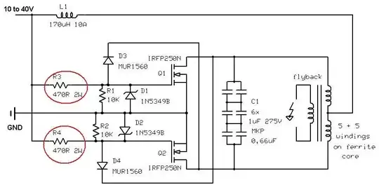
The problem are two two 470R resistors circkled in red - if gate capacitance is (say) 3nF (not unheard of by any means), the CR charging time for the gate will be: -
\$470\times 3\times 10^{-9}\$ seconds = 1.41 micro seconds. That's just 1x CR time and I suspect your circuit will take 3 times as long to turn fully on - maybe up to 5 us. Turning off is similar - it relies on the other FET turning on to kill the gate voltage and so this is going to be about the same. All this wastes a lot of power and heat. But it's worse than that because the signal on the drains I guess is going to be more resonant than switching due to L1 and the bank of capacitors.
There is also the \$\dfrac{dV}{dt}\$ voltage change on the drain affecting the gate voltage. Because the gate voltage is not powerfully driven, as the voltage on the drain starts to fall, it will, by internal drain-gate capacitance inject a signal into the gate that stops it turning on as quickly would the gate be driven by a proper drive circuit.
Like I say, I'm no expert on this type of design but it strikes me this type of switcher is good because it is simple but also inefficient also because it is too simple.