8

I've been reading up on power electronics lately and as a challenge (and also a learning exercise), designed my first switching power supply - a buck converter in this case.

My current design

It is intended to supply 3.5-4.0V (decided by diode reference source) and up to 3A in order to drive some power LEDs with any DC source, ranging from a 5V USB charger up to a 9V PP3 battery. I want an efficient supply, as heating and battery life will be a real issue (otherwise I'd be lazy and use a 7805+diode).

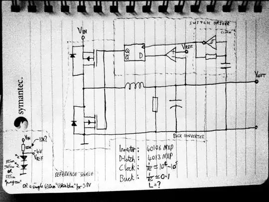
NOTE: I already noticed that I've got the switching logic the wrong way round, I need to either swap the connections into the comparator or use !Q to drive the MOSFETs.

My choice of MOSFETs instead of BJTs was due to the power losses in a BJT, and the thermal issues arising. Is this decision to use MOSFETs over BJTs/IGBTs due to improved efficiency the right call?

Rather than using a PWM chip as many hobbyist forums suggest, I decided to use a comparator/clock/latch combination to rapidly switch between "charging" and "discharging". Is there any particular disadvantage of this approach? The CMOS latch (a D-flip flop) copies data to the outputs on the rising edge of pulses from the clock generator (a CMOS Schmitt inverter + feedback).

The choice of time constants / corner frequencies for the clock and the buck lowpass (10-100kHz and 10Hz respectively) is intended to support the small ripple approximation while also allowing the output capacitor to charge in a reasonable amount of time from power-on. Is this the right set of considerations for deciding the values of these components?

Additionally, how would I go about calculating the value of the inductor? I would assume that it depends upon the typical output current and the lowpass capacitor's value, but I can't quite figure out how.

[edit:]

In the past, I've used the shown MOSFET pair (in addition to software PWM) to create H-bridges for bi-directional, variable speed motor control - and as long as I kept the PWM period much larger than the MOSFET switching time, the power waste from shorting during switching was negligible. In this case though, I'm going to replace the N-mosfet with a Schottky diode since I've never used a Schottky diode before and want to see how they behave.

I use a simple inverter+RC combo to provide the clock signal as I don't need a particularly consistent or precise frequency as long as it is considerably higher than the high-cut corner frequency of the buck-boost.

[edit II:]

  • I built it on a breadboard and to my surprise, it worked straight away without any issues, and at ~92% efficiency (compared to the 94% that I'd calculated from switching/component losses).

  • Note that I omitted the resistor in the output stage, out of laziness - also I can't quite recall why I put it there in the first place.

  • I omitted the reverse diode parallel to the P-MOSFET, and also used a 1N5817 Schottky diode (note: 1A rating) in place of the N-MOSFET. It doesn't heat enough for my fingertips to notice. I've ordered a higher-rated diode though for when I assemble the final unit, which will run with full load.

  • I accidentally blew the LM393 comparator during testing, but an LM358AN took its place straight away without any issues.

  • As I can't find any decent circuit design+layout/routing software that will run on Arch Linux x64 (or even install, in the case of native Linux software), I've manually layed it out so it probably won't work by the time it's soldered... But that just adds to the "fun" I guess!

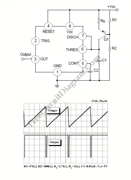
  • Component values used: Clock gen { 1kR, 100nF }; Buck output { 330uH, 47uF }; Input capacitor [not shown] { 47uF }; P-MOSFET { STP80PF55 }; N-MOSFET { Schottky diode instead, 1N5817 - to be replaced with >=3A version }; ICs { 40106 NXP, 4013 NXP, LM358AN }

Mark K Cowan
  • 285
  • 2
  • 11
  • 3
    This is a "hysteretic converter" - it relies on hysteresis at the output to provide stability (of sorts :-) ). They can work very well in practice. Many people are unfamiliar with them and some find it hard to believe that they can work well. In this case the hysteresis is provided by the inductor discharging into the output cap after the switch turns off so that Vout rises slightly above notional. ie the output ripple magnitude at the comparator input is an integral part of the operation. Look at comparator-out on a scope. It is liable to be chaotic depending on clock to time constant values. – Russell McMahon Nov 26 '13 at 22:03
  • 2
    To really blow your mins and/or open up your mental filters, remove both clock and flip flop and use comparator to drive MOSFETs directly (with due regard to drive adequacy and polarity). It works! NOW look at Comparator_out on a scope !!! | By carefulish choice of MOSFET Vgsth's you can arrange a middle dead band where one MOSFET turns off before there is enough voltage to turn the other on. You could scale voltages down with resistors but then have drive speed issues - often enough, as others say, shoot-through is low enough to be acceptable. – Russell McMahon Nov 26 '13 at 22:07
  • 1
    A very simple gate driver that has some inherent deadband can be made from a PNP/NPN bipolar pair and nothing else. Join bases. Join emitters. NPN collector to V+. PNP collector to V-. Drive input to bases. Drive output from emitters. This gives you high current drive and a ~~ 2 x Vbe middle dead band. Can add output R of a few Ohms emitters to FET gates to REDUCE gate drive current. I use BC337/327 (or BC807/817) pairs for this allowing FET gate drives of nearly an amp peak. – Russell McMahon Nov 26 '13 at 22:11
  • Thanks, I use the flip flop to buffer periodic "sign of error" values in order to determine the correction applied in the next clock cycle. I originally omitted the flipflop, but figured that the comparator would then have "continuous" feedback instead of the nearly-discrete feedback that it currently has - hence it would settle in some middle zone, resulting in the MOSFET wasting lots of energy due to being "half-on/off". In future, I will use the 2 MOSFET idea with your BJT driver, rather than the MOSFET/Schottky pair that I decided to use for this project. Thanks! – Mark K Cowan Nov 26 '13 at 22:29
  • 1
    The reason you do not get continuous feedback and linear operation is that when the FET switches off the energy in the inductor continues to deliver energy to the load and Cout and Vout continues to rise (slightly). The degree of ripple voltage from this source is part of what governs how long it takes to turn back on. Long ago I had people argue bitterly against this being adequate means of feedback control. It is :-). Switching signal is approx chaotic - very unlike what you usually see. | – Russell McMahon Nov 27 '13 at 05:14
  • 1
    If using 2 x MOSFETS with deadtime (or regardless) place a small cheap Schottky across lower FET. This will conduct as required and allows timing of bottom FET to be less critical. As the diode is only handling the leading edge switching and maybe trailing edge it can be rated far below full load current. You will see this done in even cheap chinese 12V to laptop flyback power supplies - and NOT done in the very cheapest. If you do NOT add the external Schottky the FET body diode will conduct when/if required but with high losses. – Russell McMahon Nov 27 '13 at 05:16
  • @RussellMcMahon: You know, it seems like you could make a pretty good answer just by copying and pasting those comments into the answer box... – Ilmari Karonen May 27 '14 at 22:59
  • @MarkKCowan How did this all work out for you? – Russell McMahon Sep 14 '14 at 06:41
  • 1
    @RussellMcMahon Here is the full project: http://hackology.co.uk/2013/aura/ - The final design i used is not shown there, but it had a Schottky diode in place of the lower FET and a Zener voltage reference. – Mark K Cowan Sep 14 '14 at 10:36
  • @RussellMcMahon - also note the "click to read more" link at the bottom - i need to make that more noticeable. – Mark K Cowan Sep 14 '14 at 10:41
  • @MarkKCowan Excellent - looks like fund - and a lot of work for all involved. Just skimmed through some other posts of ypurs. agh. Black Hole. Must stop. Deadline looms. Later ... :-). – Russell McMahon Sep 14 '14 at 17:16
  • @RussellMcMahon cool, which topics/posts on there interest you? Whats the deadline for? I have some crazy new stuff for the blog when i have time to write up - stuff resulting from the intersection of a physics/hacker background and severe boredom :D – Mark K Cowan Sep 14 '14 at 19:45
  • @MarkKCowan Various. On the non-technical side I liked glimpses into places I've not been. Estonia, Poland , ... . One of these days. Maybe next year and maybe never. I liked your cliche" photo (so there). And :-) - http://hackology.co.uk/wp-content/uploads/2014/04/DSC0113.jpg – Russell McMahon Sep 15 '14 at 04:35
  • @RussellMcMahon Once you get off the plane in this part if the world, travel becomes really cheap... £10 for a bus or a boat to the next country! In a 2-week trip, you can spend 3-4 days in each country from Poland to Estonia and see a lot. Travel to the next country on overnight buses so you don't lose a day for travelling. – Mark K Cowan Sep 15 '14 at 06:16

4 Answers4

5

The main problem with this schematic is that there will be a moment during switching when both MOSFETS will be conducting current and then will short the power source. As a rule, this moment is short and will not burn the MOSFETs, but the efficiency will be affected and there will be high surges in the power source.

Replace the lower MOSFET with Schottky diode in reverse.

Yes, using a MOSFET can increase the efficiency, but then the schematic needs special driver that to make dead time between switching transistors ON.

johnfound
  • 5,307
  • 1
  • 16
  • 31
  • I was just getting the same idea from answers to the question below before I read your answer! A passive switch (e.g. the Schottky diode) makes a tonne of sense now that you mention it and will also knock a quid off the total cost! Thanks! [http://electronics.stackexchange.com/questions/57468/why-does-this-buck-converter-output-such-low-current?rq=1] – Mark K Cowan Nov 25 '13 at 17:56
3

Yes, there are stability issues and a brief moment when both FETs are on but the beauty of using a FET on the pull-down part of the circuit (i.e. a synchronous buck converter) instead of a schottky diode is this: -

  1. Whatever duty cycle your PWM is the output voltage stays constant as a fraction of input voltage - you are in effect using the L and C on the output as a low pass filter to a square wave input.
  2. Whatever load you have connected, providing the FETs are lowish on resistance, within reason you don't need to change the PWM mark-space ratio.
  3. It will be more efficient on heavier loads than a non-synchronous buck regulator but the down-side is that on light loads it will be less efficient because you need current to drive the N channel FET because of gate capacitance.

I'd also advocate building a 555 timer sawtooth generator as the basis of your system. Something like this: -

enter image description here

I'd then feed it into a fast comparator and then the use the comparator output to drive the two FETs. The two FETs can be "time segregated" with a small RC time delay on the output of the comparator - the undelayed output and the delayed output would feed an AND gate for one of the gate drives and the the same for the other gate drive but using a NOR gate. Plan on maybe 50ns time delay introduced.

What you get is a half-decent synchronous buck convertor that just needs an input to the other comparator input to get the required duty cycle changes. OK so far? Then you can apply a simple control loop that lowers the 2nd input to the comparator as the input voltage gets bigger. Get this working and then apply another small control loop that actually regulates the PWM with load current changes a tad and this would probably work and no negative feedback involved.

Then, as the final touch, and with care and subtlety apply an overall control loop to keep the output better stabilized but remember, with a sync buck you can pretty much get half-decent stable performance without control loops that use negative feedback - if you are wanting to go this approach I can recommend it.

However, for me, I'd just call on Linear Technology and get the device that already does the job.

Andy aka
  • 434,556
  • 28
  • 351
  • 777
  • I'm curious as to what advantage the 555 circuit would have over my inverter design in this application - the actual oscillation frequency can be off by almost an order of magnitude without causing much of a problem so the 555's precision isn't needed, also the 555 circuit has a higher part count. While I'd typically rather use two MOSFETs (with a pwm period considerably longer than the MOSFET switching time), I've gone for Schottky diode simply as I've never used one before and want to see how it behaves. My past power switching devices (motor controllers) still work fine with two MOSFETs. – Mark K Cowan Nov 25 '13 at 21:13
  • Also, while the Linear Technology devices are almost certainly more precise than my design they have a similar part count, and I'm partly doing this as a learning excercise (hence no fancy single-chip PWM driver). I'll add `Linear Technology` and their site to my notebook though, thanks! – Mark K Cowan Nov 25 '13 at 21:26
  • 3
    @MarkKCowan The whole approach is debateable other than as a learning exercise so not knowing what you wanted to learn I threw in the 555 idea but there is an important reason behind it. Your oscillator produces a squarewave but you can use the voltage on the capacitor but it is (A) a non-linear ramp and (B) has undefined thresholds of amplitude that may drift as the device warms up but listen dude, you do it how you feel is right. Non-linearity and unpredictable thresholds - just remember where you heard it first LOL. – Andy aka Nov 25 '13 at 22:19
  • 1
    The 555 circuit is used to produce a nice smooth ramp for the PWM generation. It is not used for its frequency accuracy; it allows you to turn an analog voltage into a smoothly varying duty cycle. – alex.forencich Nov 26 '13 at 07:11
  • Another feature of synchronous converters (which may or may not be an advantage) is they can transfer power in both directions. Handy if you want to do regenerative breaking. – Peter Green Mar 04 '16 at 05:09
2

I use to calculate smps at http://schmidt-walter.eit.h-da.de/smps_e/smps_e.html

I already designed flyback as well as buck converters for LED lighting using this website, and it was every time the best solution. You find there the dimension for the coil you need (core & winding).

Nick Alexeev
  • 37,739
  • 17
  • 97
  • 230
  • I've been planning on using my physics background to create some SMPS-designing program when I get the time... Thanks for that site, it's a goldmine of ideas! – Mark K Cowan May 28 '14 at 10:04
1

I think a better approach to generating the PWM signal is to actually build a proper control loop. It's not clear to me that your circuit will actually stabilize where you want it to.

What you should do is build a simple P or PI controller. Take your output voltage and your reference voltage and put them through a differential amplifier to get an error voltage. Then run this through a potentiometer so you can adjust the gain. If you want to make it more accurate, run it through another pot, an integrator, and then put both of these into a summing amplifier. This will give you an output that is proportional to the error and to the integral of the error, with adjustable gains. Then you run this to one input of a comparator. The other input of the comparator would be triangle wave from a relaxation oscillator. The output of the comparator would drive the MOSFETS, possibly with a MOSFET driver and perhaps some additional logic to prevent shoot through. You'll have to play around with the potentiometer settings to get the best result.

alex.forencich
  • 40,694
  • 1
  • 68
  • 109
  • Sounds interesting. Why would I compare the error to a triangle wave though vs. using the sign of the error directly? – Mark K Cowan Nov 25 '13 at 21:23
  • 1
    The idea is that it will generate a nice PWN signal. You don't want to only look at the sign of the error, you want to look at how much it is off by. The correction when you are off by 1% is very different from when you are off by 50%. If all you look at is the sign, you will get strange results. Also, the triangle wave will be compared to an amplified version of the error signal. Without the integrator, the voltage will droop slightly under load as the required level to generate the required duty cycle will be lower. The integrator will clean up this error on a longer time scale. – alex.forencich Nov 26 '13 at 07:09
  • @alex.forenich: Thanks, I'll model that mathematically later - interesting! This is my first question on electronicsSE and I've already learnt a lot! – Mark K Cowan Nov 26 '13 at 11:49
  • There are numerous potential topologies. He has made a "hysteretic converter" and they work well in practice. (I have a design using one in its power supply which was produced in substantial volume commercially). – Russell McMahon Nov 26 '13 at 21:58
  • @RussellMcMahon: Hypothetically, if I was to be totally anal about efficiency for a DC-DC power converter with inputs and outputs both below 30V (no particular values in mind), what topologies would you suggest? – Mark K Cowan Jan 21 '14 at 18:29
  • 1
    @MarkKCowan - The synchronous buck converter topology (with high and low side switches) that you have or had is probably as good as any if Vin is not vastly less than Vout. For very large differences - say 4:1 + you may be better with a converter that downconverts followed by a buck stage - this can still use a single switch with the buck converter being "passive". But for what you are doing this looks good. At high currents the lower FET rather than a diode can make a substantial difference. I recently bought a cheap Chinese 24V to 12V @ 20A out converter and last night pulled it apart to ... – Russell McMahon Jan 22 '14 at 10:10
  • 1
    ... see what they did. It uses a TL494 plus 2 parallel FETs as the upper switch (to get the required current rating) and a dual Schottky lower diode. This is rated at about 0.6V drop at 20A or 12W @ 240W out (12 x 20A) or 5% efficiency loss just in the diode. Diode Reffective = V/I = 0.6/20 = 30 milliOhm. While that is a reasonable result a FET at 10 milliOhm would be easy to get and 5 or even 1 milliOhm FETs are available at not utterly bank breaking prices. A 5 mO FET takes 'diode' loss down from 5% to under 1%. ... – Russell McMahon Jan 22 '14 at 10:16
  • 1
    ... | Using an optimised controller and proper driver would help BUT the cheap 2 transistor driver does an OK job. You should be able to get 95% real world efficiency in many cases and in some quite challenging high power applications people claim 98% +. Such high efficiencies usually are at some optimised mix of Vin, Vout and power - move away from the optimised design point and it drops off. You can see this in many data sheets and app notes where one curve will peak at 95% + but you can expect much less elsewhere on the operating 'landscape'. – Russell McMahon Jan 22 '14 at 10:19
  • 2
    Using a FET alone as the bottom switch means the switching timing must be 'just right'. By paralleling a lower rated Schottky across the lower FET the diode will deal with edges that aren't timed quite right and the FET handles the bulk of the current x time. The Schottky can be much lower rated than if it was used alone as it only handles transient events at one or both ends of the on period. – Russell McMahon Jan 22 '14 at 10:22
  • @RussellMcMahon: Wow, thanks! I probably should have put that as a separate question so I could accept your detailed and clear answer for it! – Mark K Cowan Jan 22 '14 at 19:00