97

In low-cost mass-produced items I often run into black blobs of what looks like resin applied directly on top of something on the PCB. What are these things exactly? I suspect this is some kind of custom IC that is layed out directly on the PCB to save on the plastic housing/connector pins. Is this correct? If so, what is this technique called?

The Blob

This is a photograph of the inside of a cheap digital multimeter. The black blob is the only non-basic piece of circuitry present, along with an op-amp (top) and a single bipolar junction transistor.

drxzcl
  • 3,735
  • 2
  • 30
  • 32
  • 8
    If you really want to know more, you can dissolve the epoxy and have a look http://travisgoodspeed.blogspot.com/2009/06/cold-labless-hno3-decapping-procedure.html – Toby Jaffey Jan 17 '11 at 17:40
  • @Joby - I've never tried it, but I imagined that the epoxy is a different sort of component from the plastic cases. Now I need to get myself some acid and try it out.... – Kevin Vermeer Jan 17 '11 at 21:19
  • 11
    That picture is really funny in that rather advanced manufacturing like COB is used, but it's surrounded by archaic thru hole discrete resistors and even a 8 pin DIP. – Olin Lathrop Nov 22 '11 at 16:37
  • 3
    To top it off, the 8-pin DIP is a 741! – drxzcl Nov 22 '11 at 19:02
  • 7
    Chip on board is hardly "advanced" - it's been around for ages. – Chris Stratton Nov 23 '11 at 04:26
  • I always thought it was a secrecy thing, to stop punters being easily able to see what was going on with the circuits. That's how it felt to me when I was a curious kid ripping apart calculators, anyway. – deed02392 Aug 15 '13 at 22:03
  • I first saw chip-on-board inside a digital watch in 1970-something. – Kaz Jan 15 '16 at 17:08
  • If someone is interested in the manufacturing process for the chip-on-boards, here is a link: [How Chip-On-Boards are Made](https://learn.sparkfun.com/tutorials/how-chip-on-boards-are-made). [Just piling up references.] – Nick Alexeev Aug 12 '17 at 23:06
  • https://www.pcbjhy.com/metal-core-pcb/57132185.html – Brian Cannard Apr 18 '20 at 00:21

4 Answers4

77

It's called chip-on-board. The die is glued to the PCB and wires are bonded from it to pads. The Pulsonix PCB software I use has it as an optional extra.

The main benefit is reduced cost, since you don't have to pay for a package.

stevenvh
  • 145,145
  • 21
  • 455
  • 667
Leon Heller
  • 38,774
  • 2
  • 60
  • 96
  • 8
    This is exactly what I needed! Searching for "chip-on-board" yielded a wealth of information, including a page that shows the various stages of assembly before the "blob" is added. http://www.empf.org/empfasis/dec04/improve1204.htm – drxzcl Jan 17 '11 at 16:25
  • 3
    Also called glob-top or blob-top http://en.wikipedia.org/wiki/Blob_top . – davidcary Jan 17 '11 at 17:44
  • 2
    You may also want to look into "potting" (http://en.wikipedia.org/wiki/Potting_%28electronics%29). Encapsulating the die in resin may also have security advantages -- the chip(s) under it require quite a procedure to expose and identify. – Saar Drimer Jan 17 '11 at 23:45
  • 1
    @Davidcary very interesting. I am sure @Ranieri had no ideal that "blob" was actually the technical word for it when asking the question. – Kellenjb Jan 18 '11 at 02:43
  • @Kellenjb: I certainly did not! But it is very descriptive and engineers have a way of calling a spade a spade. Or a TLA ;) – drxzcl Jan 18 '11 at 22:34
  • 1
    CoB was invented because electronics people were jealous of how computer programmers were able to inline code with just a textual macro or a compiler declaration. They wanted the same thing, but for an entire chip, to do "one better". – Kaz Jan 15 '16 at 17:13
40

It is a "Chip on board". It is an ic wire bonded directly to the board, and then protected with some epoxi (the "black thing").

enter image description here

enter image description here

Wesley Lee
  • 7,844
  • 6
  • 35
  • 53
40

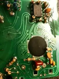
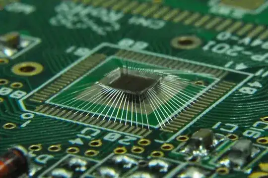
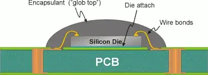
Like Leon said the techniques is called Chip-on-board (COB). You do exactly the same to bond the die directly to the PCB as you would to bond the pins in an IC package. Savings: no package needed. (You could say no soldering also, but that has to be done anyway, so that's not really something you save on).
COB is not cost-effective for small series, and with a few exceptions you will only see it on mass-produced products (100k~1M/year).
The blob is an epoxy resin to protect the IC with the bonding mechanically; the bonding wires are very thin (as thin as 10\$\mu\$m for gold wire) and therefore extremely fragile. Another form of protection it offers is reverse engineering protection. This is not fool-proof (the resin can be removed), but it's a lot harder to reverse-engineer than simply desolder an IC.

IP protection example: until a few years ago FPGAs always needed an external serial memory to load their configuration from. This configuration could be an almost complete product design, and therefore expensive. Yet, simply by tapping the communication between FPGA and configuration memory everybody could copy the design. This can be avoided by COB-ing FPGA + memory together under a single epoxy blob.

note: the die in a BGA is also bonded on a thin PCB, which routes the signals from the edges of the die to the ball grid at the bottom. This PCB is the base of the BGA's package.

stevenvh
  • 145,145
  • 21
  • 455
  • 667
11

I know this is an old question, but there is one aspect of COB that was not mentioned. The issue is that you must start assembly with Known-Good-Die. IC components are nearly always tested after they are packaged. It's simply easier to handle a packaged component than it is to place tiny probes on the unpackaged chip. This is a problem for COB because if you place an untested chip, you potentially have to throw away an entire assembly if that chip turns out to be bad. So, COB usually must use KGD. The chip testing is usually done at the wafer level, before the die are diced (sawn apart). Unfortunately this testing is usually slow and expensive (relative to testing in packages) so this consumes some of the potential cost savings of COB.

user6672
  • 141
  • 1
  • 3
  • 4
    I don't agree. Testing chips in a wafer using flying probe is easier than testing packages chips. Granted, the probes' precision must be much higher, but that technology is readily available. And testing on the wafer is *much faster*; you can go from one die to the next in a fraction of a second. – stevenvh Nov 22 '11 at 16:54
  • 2
    Economics could be such that they test them after they are on the boards (but maybe before other components are installed). Unfortunately, that would increase the e-waste to be disposed of. – Chris Stratton Nov 23 '11 at 04:31