simulate this circuit – Schematic created using CircuitLab
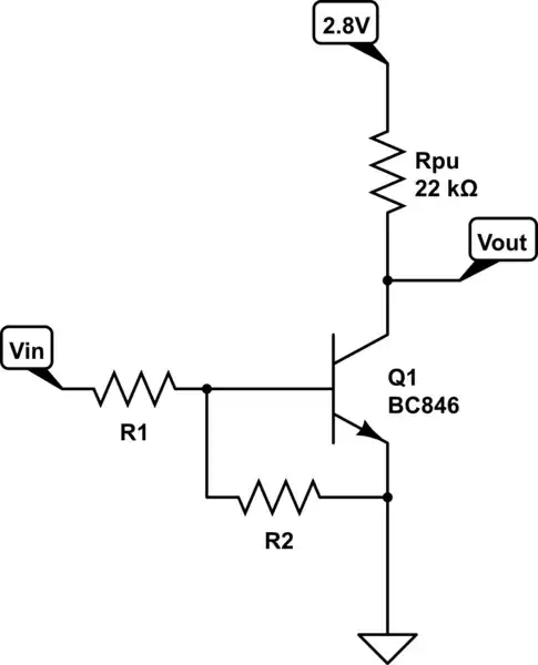
In above circuit the base of Q1 acts as a level-shifter from 3V-50V at it's base to 2.8V. The base of Q1 is driven by PNP open-collector outputs thus R2 holds the Q1 in it's off-state when the input signal is not asserted. The output pull-up can be rather large (22k) since speed is not too important but power-consumption is.
This gives a collector current of:
$$ I_{C(min)} = \frac{2.8\mathrm{V}}{22\mathrm{k\Omega}} = 0.13\mathrm{mA} $$
This leads to a small required base current, even when underestimating the current gain and providing a 30% error budget:
$$ h_{FE(min)} = 100 \\ V_{BE(sat)} = 0.75\mathrm{V} \\ I_{B(min)} = 1.3 \frac{I_{C(min)}}{h_{FE(min)}} = 0.0017\mathrm{mA} $$ As noted above the input voltage at the base relative to ground is in the range of \$V_{in(min)}=3\mathrm{V}\$ to \$V_{in(max)}=50.4\mathrm{V}\$ which imposes the following restrictions on \$R_B\$:
$$ R_{1(max)} = \frac{V_{in(min)} - V_{BE(sat)}}{I_{B(min)}} = 1.3\mathrm{M\Omega} $$
According to those calculations \$R_1=1\mathrm{M\Omega}\$ and \$R_2=10\mathrm{M\Omega}\$ would be sufficient.
However, I wonder whether there are any drawbacks choosing resistors in the Mega-Ohm range for transistor biasing.