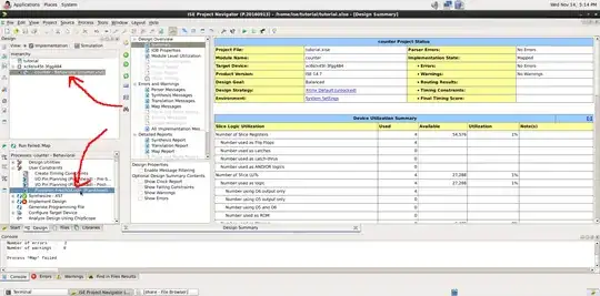
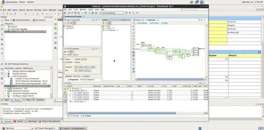
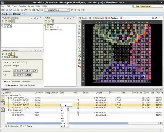
Recently I started learning FPGA programming. I have the " Verilog QuickStart book" and downloaded Xilinx ISE Webpack v14 and watched a number of YouTube videos. At this moment I can build my circuits and test them by the inbuilt simulator but I don't know how to assign the physical pins of the FPGA ( the I/O buffers).
For example let's assume we have a very very simple design: just an AND gate ( Module ports include IN1, IN2 and OUT). It is easy to make the circuit on the software but assume I want to assign the IC I/O pin number 7 as IN1, pin 9 as N2 and pin11 as OUT ( all I/O ports without VREF) . Nowhere in the software (as well as the book) I saw how to do this assignment.Can anyone help me on that please?
Any help appreciated in advance.


