5

It just strikes me as very odd that all representations of the actual physics of NPN transistors in textbooks is perfectly symmetrical, yet neither the diagram used to represent them nor the mathematical model used to simulate them seem to reflect that.

Could someone explain where and how the symmetry disappears when going from the physical model to the mathematical one ? Is that asymmetry not important enough that it's just not worth depicting it ?

Here's an example of what I mean :
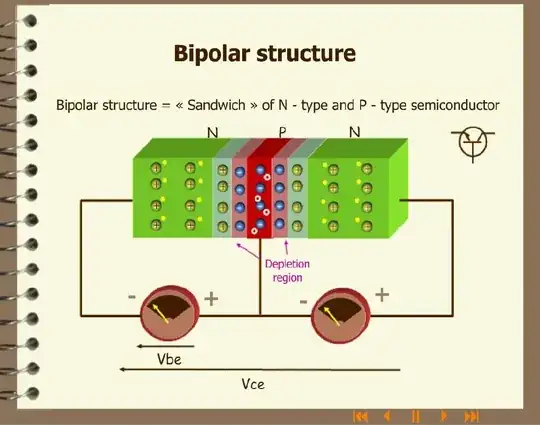
Bipolar structure
(source: ustudy.in)

Glorfindel
  • 1,245
  • 3
  • 15
  • 20
blondiepassesby
  • 757
  • 7
  • 18
  • 2
    It's a bit like the map of the London Underground tube system. Excellent for a general guideline but poor at giving relative distances between stations. – Andy aka Oct 28 '13 at 21:30
  • See http://commons.wikimedia.org/wiki/File%3aSmall_Transistor_Metal_1.jpg – RedGrittyBrick Oct 28 '13 at 23:13
  • @RedGrittyBrick : my question is different from the one you quote, but the explanation given in the most voted up answer is exactly what I was looking for. Thanks ! – blondiepassesby Oct 29 '13 at 00:23

1 Answers1

3

The design of the schematic symbol does not represent the actual geometry of the semiconductors' (n- and p- types) being used. Rather, it is derived from the original bipolar junction constructed by John Bardeen and Walter Brattain.

You should also note that in a bipolar junction transistor, the outer n-type semiconductor in a NPN (or p-type semiconductor in a PNP) may not necessarily have the equal concentrations. They could also have a completely different construction than the one shown in your screenshot. But the primary construction is, indeed, two semi-conducting materials of the same type (but not necessarily of the same charge concetration) being physically separated by a layer of semiconducting material with charge concentration opposite that of the outer semiconducting materials.

Shabab
  • 414
  • 2
  • 9