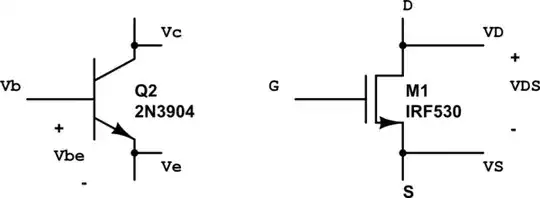
For the BJT in cut-off, why do we have to assume \$V_{ce}>0\$?
If the NPN is in cut-off (as defined by very low base current \$I_{b}\$), its C-E behaves as an open circuit, so its voltage will be determined by whatever it is connected to, be it negative or positive (so \$V_{ce}>0\$ is not required).
However, if the external circuitry tries to make \$V_{ce}\$ negative, \$V_{bc}\$ may become positively biased and \$I_{b}\$ will increase by flowing to the collector. In this case the BJT will no longer be in cut-off, and the behavior will be as if the C-E terminals were reversed, but with much lower performance, breakdown limits, and overall specs.
The following graph should help:
(source)
Also, see BJT in Reverse Active Mode of Operation for a related discussion.
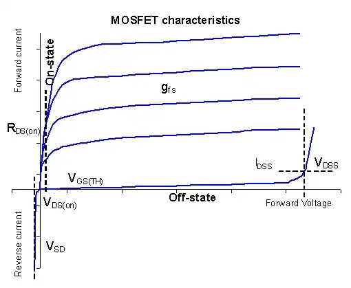
For the MOSFET in cut-off, why do we have to assume \$V_{GS}<V_{th}\$ and \$V_{DS} > 0\$?
\$V_{GS}<V_{th}\$ pretty much defines the cut-off region (very little current will flow), and \$V_{DS} > 0\$ is required because if it is sufficiently negative, current will flow via the body diode from source to drain. So the condition should really be \$V_{DS} > -Vdiode\$.
This graph should help you visualize this behavior: