There are some base assumptions here that was covered in another post (which I can't find now).
If you count the total number of placed logic elements and clocked logic (total number of FF's shipped) they are probably going to be in processor and microprocessors, Intel, DEC etc. The manifestation of this is that you end up with a small groups of people/teams who are responsible for designs covering many decades, with not a lot of details of the internal workings.
Conversely you have many different teams working on ASIC flows, with many more projects but corresponding less volume.
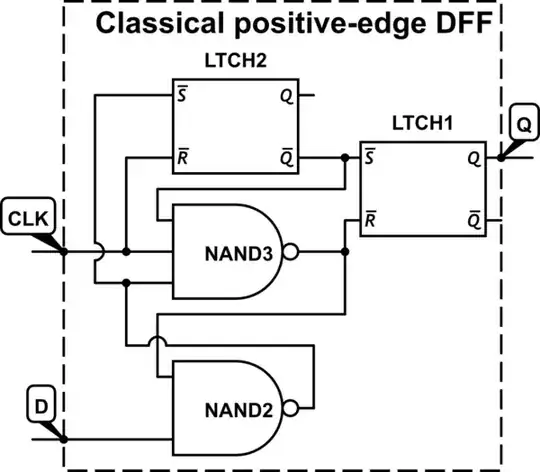
Most processor designs are actually not positive or negative edge clocked but are designed using a double latch, NOC (Non Overlapped Clock) complimentary clocking scheme.
So you end up with a inputs -> (logic cloud) -> latch from clock -> logic cloud -> latch from !clock scheme. Which is the canonical form of a master slave FF with logic stuffed inside.
This sort of design methodology has several advantages but also has additional complexity.
Another unfortunate thing is that this design methodology is not taught in most universities. All of the Intel x86 designs are of this sort (one must not confuse external operation of interfaces with internal operation) with the notable synthesizable SOC cores that they have been designing for mobile handsets.
An excellent discourse on this can be found in "Dally, William J., and John W. Poulton". Digital Systems Engineering. Cambridge University Press, 1998. section 9.5 discusses "open loop synchronous timing" <-chapter title. But to quote "Edge-triggered timing, however, is rarely used in high-end microprocessors and systems designs largely because it results in a minimum cycle time dependant on clock skew".
Yes, a totally pedantic answer. but an important methodology that is little known, considering how many total transistors are out there in these designs (lots and lots).