I need a trace on my PCB to carry up to 2.5 amps (average) current, with 5-6 amp spikes (it's going to a switch mode power supply.) How wide should the traces be? I've got a trade off between reliability and size, as the product is space constrained. Any tips would be appreciated.
Asked
Active
Viewed 4.3k times
4 Answers
24
After doing a quick google of "PCB Current Calculator", I found a PCB Current Calculator based on IPC-2152. It bases the width of the track on how much of a temperature rise the trace is allowed to have. It's nice in that it shows how much power you waste through your trace. I would design for your worst-case RMS current, since it's going to be a periodic signal.
If you use 2 oz/ft2 copper instead of the standard 1 oz/ft2 copper, you won't need as wide of a trace to achieve the same resistance. For example, allowing for a 10 oC rise, you can get away with these numbers at 3 A with no copper plane nearby:
- 177 mil (4.50 mm) on 1/2 oz/ft2 copper
- 89 mil (2.26 mm) on 1 oz/ft2 (35µm) copper
- 47 mil (1.19 mm) on 2 oz/ft2 (70µm) copper
Note: IPC-2221 (The standard used in the original answer) uses old measured values for its design charts, and these charts are implemented in many calculators. As best as I can tell, this data was claimed to be 50 years old, which makes IPC-ML-910 (1968) a possible source. As @AlcubierreDrive pointed out, a new standard, IPC-2152, contains new measured data, and presumably is more accurate. More importantly, a comparison of IPC-2221 values gives the following result for trace widths: IPC-2221 (internal) > IPC-2152 > IPC-2221 (external). Actual numbers for the example above (1oz copper) are
IPC-2152:             89 mil
IPC-2221 (internal): 143 mil (+60%)
IPC-2221 (external):  55 mil (-38%)
Also note that the original numbers in this answer were based on the IPC-2221 internal calculations, which will provide a conservative estimate for all values.
W5VO
- 18,303
- 7
- 63
- 94
-
*This calculator is incorrect!* It is based on IPC-2221, which is *incorrect* and has been superseded by IPC-2152. Using IPC-2221 *will result in undersizing your outer layer traces by a factor of 2!!* For historical background, google IPC-2152, or see the section titled "The Historical Chart" in this document: http://frontdoor.biz/PCBportal/HowTo2152.pdf – AlcubierreDrive Jan 22 '16 at 06:17
-
@AlcubierreDrive Interestingly, this was written around the time IPC-2152 came out. I'll update my answer accordingly. Do you know if the more recent IPC-2221B (2013) addresses this issue? – W5VO Jan 22 '16 at 16:23
-
[NinjaCalc](http://mbedded-ninja.github.io/NinjaCalc/) includes a track current calculator based on the IPC-2152 standard. Disclaimer: I am the author. – gbmhunter Mar 30 '16 at 03:19
21
Common practice for high-current devices is to solder thick copper wire on top of your 2-3mm trace. 1mm^2 wire can handle 10A easily.
BarsMonster
- 3,267
- 4
- 45
- 79
9
I remember having seen this nomogram in another answer:
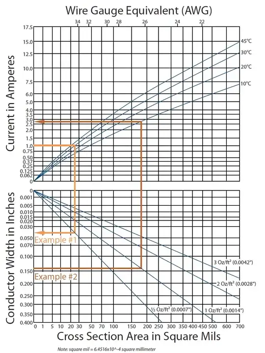
Select 2.5A on the vertical axis of the top graph. Move to the line indicating the allowed temperature rise. Move downward to the PCB's copper thickness in the bottom graph. This intersection gives you the required width on the vertical axis.
-
You probably mean this answer: http://electronics.stackexchange.com/a/5405/4950 – PetPaulsen Apr 13 '12 at 08:17
-
2
Another option would be to use PCB Busbar soldered into the PCB - they would also add some nice rigidity to your PCB should it need it
BullBoyShoes
- 928
- 4
- 5
-
-
1@stevenvh - What? No they're not. Plus, a buss-bar is generally perpendicular to a PCB, so it is **far** more rigid. In fact, [they're actually sold **specifically** as PCB stiffeners](http://www.cci-msc.com/Rigidbus/index.html). – Connor Wolf Apr 13 '12 at 09:02
-
@Fake - Yes, I've seen them sold as stiffeners, but I'm not sure that's a good idea: you want as little force as possible exerted on soldering connections. – stevenvh Apr 13 '12 at 09:08
-
@Fake - just asked [this question](http://electronics.stackexchange.com/questions/29828/are-board-stiffeners-ok) about it. – stevenvh Apr 13 '12 at 09:22