3

I'm trying to design a pulse induction metal detector to increase my EE skills a little bit.

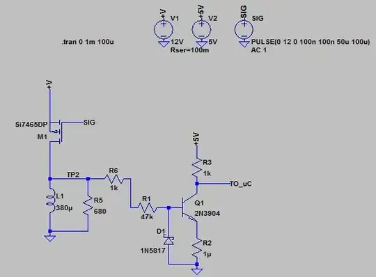
I started to sketch out the transmitting stage, which is just a MOSFET that switches current through a search coil and limits the back-emf for further processing.

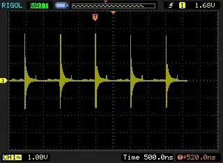
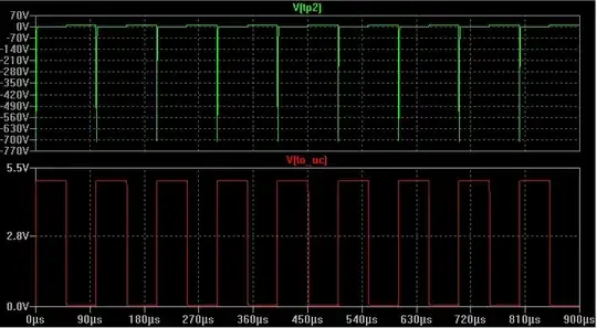
What I want to achieve is to pull a pin on my microcontroller high (+5V) when the transmit pulse starts and pull it back to low (GND) when the back-emf sets in i.e the voltage goes negative on test point 2 (TP2).

The microcontroller pin is therefore connected to test point 3 (TP3) and the problem I have is that the transistor is still open (?) and the voltage drops to -12V, which kills the input pin on the microcontroller.

So my question is how could I improve the design to only have +5V or GND on the microcontrollers input pin? I've already tried to place a diode after the emitter but this still leaves a negative voltage of about -0.7V ...

Thanks for any advice!

PS: The TVS diode clamps the voltage to +/- 12V

Schematic Testpoints


RESPONSE TO ANSWER

Updated schematic

sled
  • 249
  • 2
  • 8

2 Answers2

3

As Andy says the large negative pulse will break down the base-emitter (and damage the transistor), they are typically rated for ~5V reverse maximum.

The idea you have isn't so bad, with a couple of component value changes it can work. Basically you need to increase the impedance going into the base, add a protection diode across the b-e junction, and lower the impedance at the output of the transistor (this makes it less susceptible to anything working against it, noise, etc)

Also when simulating coils remember to include any coil resistance and parallel capacitance - this can make a big difference to your simulation (i.e. the reverse EMF will likely be much lower in real life if it's a big hand wound coil - if you have a LCR meter use it to get some measurements)

Something like this (I just took the relevant bits) is a start. Obviously the 1k and 47k resistors can be just one, I was following your schematic and was going to add the other bit but decided against it. The output to the uC is inverted but this it trivial to compensate for in firmware (or you can take the output from the emitter still if you prefer, with a lower resistor value):

enter image description here

Simulation:

enter image description here

One last thing - your uC input will tolerate a small negative voltage and will likely have some input protection (the details will be in the datasheet) so up to around -0.3V or so will probably be okay.

Oli Glaser
  • 54,990
  • 3
  • 76
  • 147
  • thank you very much for your detailed explanation! May I ask if the anti-parallel diodes (D3, D4) are still needed? As far as I understand the voltage gets clamped by protection diode across the B-E junction, right? My intention is to grab the clamped signal from the base and feed it to an op-amp :) – sled Sep 28 '13 at 23:01
  • D3/D4 (or similar) are still needed if you wish to limit the opamp input, yes. If you take the opamp signal from the junction of R1/R6, then the 47k resistor (R1) effectively isolates the clamping effect from this junction (i.e. it will still see the large negative swing - simulate it and check for yourself. Due to R1, the Q1 portion has almost no effect on the rest of the circuit) So I would treat the opamp portion separately and design accordingly. – Oli Glaser Sep 28 '13 at 23:09
  • hi, I tried that (see my updated question) but when I add the anti-parallel diodes at the junction between 1k and 47k resistor, it seems like the voltage drops across the diode and the transistor does not switch so that the "to_uc" node is always at ~5V :( – sled Sep 29 '13 at 00:01
  • Sorry, I wasn't clear - if you are doing it like this you need to also "isolate" the diodes in the same way as the transistor. Placing a similar value resistor (e.g. 47k) between the junction and the diodes will stop them affecting the transistor. – Oli Glaser Sep 29 '13 at 00:09
2

I think the large negative back emf from the coil is actually breaking down the base emitter region of Q1.

Why don't you take the MCU signal from the output of U1? There may be a slight delay (about a microsecond or less) before the real pulse has got across the coil but you can factor this in with a micro no problem.

Andy aka
  • 434,556
  • 28
  • 351
  • 777
  • hi, the problem with the delay is that the sampling window is about 10 microseconds after the back-emf. The goal is to measure the induced voltage curve (uV to mV) from the eddy currents after the spike has decayed to a certain level. Therefore I want to start a short timer as soon as the back-emf sets in and start the sampling when the timer has timed out. – sled Sep 28 '13 at 22:00
  • @sled so start the timer and wait a bit longer. From the end of the drive pulse to the real point at which the back-emf starts is going to be a fraction of a micro second and constant and if it isn't constant then there's something wrong or your MD is sat over a chest of gold. Maybe you can link a document that says otherwise. – Andy aka Sep 28 '13 at 22:57