I am currently studying solid state electronic devices and want to build my concept in this subject. Can anyone explain to me what is E-k Diagram and what is its significance?
Asked
Active
Viewed 6.7k times
7
-
7For those who tagged this "unclear what you're asking"... It seems perfectly clear to me. OP narrowed the topic area to "solid state devices". There's really only one E-k diagram that's discussed within that topic. So what's not clear? – The Photon Sep 28 '13 at 17:18
-
1I'll second what @ThePhoton said! on top of that, while you could move this over to Physics.SE most research in universities in this area is done in EE departments, it certainly belongs here. – placeholder Sep 28 '13 at 17:36
1 Answers
10
An E-k diagram shows characteristics of a particular semiconductor material. It shows the relationship between the energy and momentum of available quantum mechanical states for electrons in the material.
First, consider a basic E-k band diagram like this one (the x-axis can be either momentum, \$p\$, or wavenumber, \$k\$, since \$p=\hbar k\$):
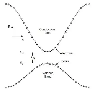
(image source Best Innovative Source)
In this diagram you can see a few things:
The band gap (EG), which is the difference in energy between the top of the valence band and the bottom of the conduction band.
The effective mass of electrons and holes in the material. This is given by the curvature of each of the bands.
This diagram indicates (diagramatically) how the actual electron states are equally spaced in k-space. Which means that the density of states in E (\$\rho(E)\$) depends on the slope of the E-k curve.
There is a more complex form of E-k diagram that shows the relationship for different directions of k relative to the crystal lattice:
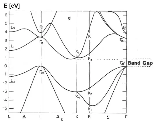
(image source: University of Kiel)
Here, the greek letters (\$\Gamma\$, \$\Delta\$, K, etc.) on the x-axis indicate different directions of k relative to the crystal axes.
In addition to showing the effective mass at different band extrema, this also shows that the effective mass varies depending on the direction of conduction relative to the crystal orientation.
This type diagram also shows whether the material is a direct-gap or indirect-gap semiconductor. Direct gap is when the valence band maximum and conduction band minimum occur at the same location in k-space. This is important in optoelectronics because only direct gap materials (like GaAs, but not including silicon) have efficient radiative absorption and emission, which is what makes LEDs and laser diodes work.
Sparkler
- 803
- 1
- 12
- 29
The Photon
- 126,425
- 3
- 159
- 304
-
Just as a note - Si makes an excellent Photodiode material and it is a indirect bandgap material - so you may want to revisit your last sentence. How the indirect bandgap affect Si as a PD is that it has a wavelength dependance upon absorbtion depth. Good answer, I'll +1 later! – placeholder Sep 28 '13 at 17:34