I will interpret this question as "why does changing the Gate Oxide thickness modulate the S/D leakage current" i.e. why does the effect exist in the BSIM model, what are the physical processes involved in this occurrence.
This is a paradoxical result (explained later) and arises from the extreme scaling effects of small transistors.
Summary: Barrier lowering from short channel effects due to the design of the transistor. This barrier lowering reduces the effective \$V_{TH}\$ which increases the \$I_{DS}\$.
Housekeeping: The OP has not stated enough information in order to answer this question so I will state my assumptions and reasons for these assumption first.
I am assuming that these are pocket (i.e. halo implanted - more details later) transistors.
This is a reasonable assumption because at any process node below 180 n you can't get enough gate control or yield from a non-pocket transistor.
we also have hints that this is concerning small transistors because the OP is dealing with BSIM 4 which came into existence for transistors in process nodes of 90 nm and below.
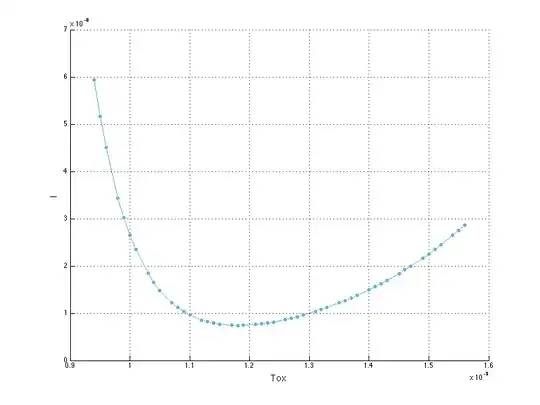
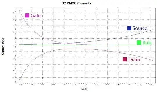
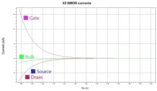
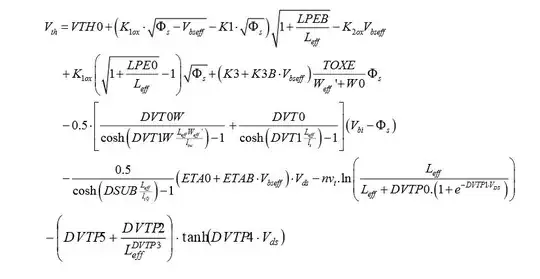
we also see the \$I_{DS}\$ modulation with \$T_{ox}\$ effect that implies a maximum \$V_{TH}\$ which decreases with changes in effective channel length away from an optimal. This is classical pocket transistor behaviour. Classical long channel MOS FET cannot behave that way.
and the oxide thicknesses are in the range of oxides used (unknown material however) in process nodes that are in 65 nm and below range.
Attribute for copied images are in the image descriptor in source.
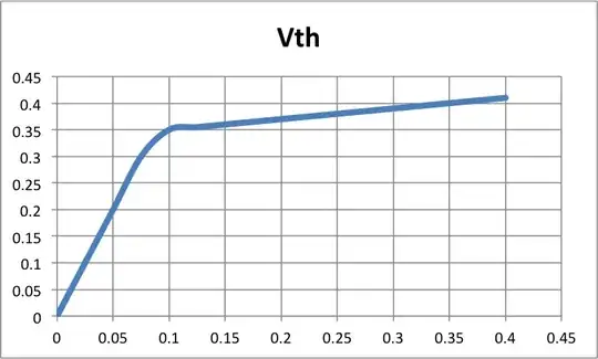
If you have a long enough transistor (i.e. S/Ds do not influence the channel) there is no expectation that a change in \$T_{OX}\$ should change the the \$V_{TH}\$. The threshold will be affected by the work function of the gate, the doping level of the channel/Well, surface traps and fixed charge in the Oxide. This is evidenced by a classical dependance of \$V_{TH}\$ curve seen below. The Threshold voltage is a flat line as the length increases.
But clearly this effect is happening in smaller transistors. To understand this you have to understand some of the design details of modern transistors. In order for short transistors to work they must have the following characteristics as shown below. (I've mangled the data a bit to quickly get it into excel - my apologies)
 \$V_{TH}\$ vs. Physical Length - [V vs. um] c/w halo implant
Underneath the the S/D implants are some specialized implants called halo implants which increase the well doping locally in front of (towards the channel side) the S/D implant.
Without the Halo implants the transistor at these small dimensions would have the following characteristics.
 \$V_{TH}\$ vs. Physical Length - [V vs. um] w/o halo implant
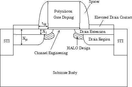
With a Halo implant, the channel is no longer uniformly doped along it's length. The surface charge density varies with position. The end result is that the transistor is much more manufacturable. In the second drawing above you will see that if the channel length is modulated (say through LER - Line edge roughness) that the transistor stays at roughly same threshold. So process variations around a nominal gate length will yield nominal \$V_{TH}\$ the third drawing (without Halo) shows an increasing \$V_{TH}\$ for longer channel lengths and more variation of \$V_{TH}\$ with change in L.
It also helps reduce the influence of the S/D on the channel and gives the gate more control. This means that the S/Ds can be brought close together without adversely affecting the \$V_{TH}\$ . Thus the transistor is smaller (but do keep in mind that 10's of nm are being fought for here). As an aside, this now necessitates new implants like a APT (Anti-Punch-Through) implant to prevent the S/D from joining depletion regions together under the channel. But that is another story.
The physical model is thus: As \$T_{OX}\$ increases the gate loses some of it's control over the channel. The fringing fields from the gate in the sidewalls/spacers above the LDD extensions does not have as much ability in its fight with the S/D implants for control of the channel, that lowers the barrier which effectively lowers the \$V_{TH}\$.
I recommend getting "Tsividis, Yannis". Operation & Modeling of the MOS Transistor. 2nd ed. McGraw-Hill Companies, 1998. (probably a newer version would be better) for any one at all interested in transistor physics. From that edit, page 263 here is a scan:
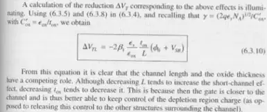
This discusses the modulation of \$V_{TH}\$ with length. In particular the \$ \frac{t_{ox}}{L}\$ term is very interesting. It says that length modulation is the same as oxide thickness modulation. Here the question is what is happening with thickness change, the answer is the gate is surrendering control. The same effect of the same magnitude can be obtained with a length modulation. It is totally about the fight between the S/D control of the channel vs. the Gate control of the channel.
- as an aside -> test the model -> increase the length at the same time you are increasing the oxide thickness in your models.
This effect is related to DIBL - (Drain Induced Barrier lowering) which arises from the drain region depletion region expanding because of higher voltage which then starts to take over control the channel.
This is a complex subject, it is not covered in text books, but in research and published articles and I have hardly done justice to the nuances involved.