10

I am working as a winter intern at a robotics company. My job is to assist the lead embedded developer in... whatever he wants my assistance in.

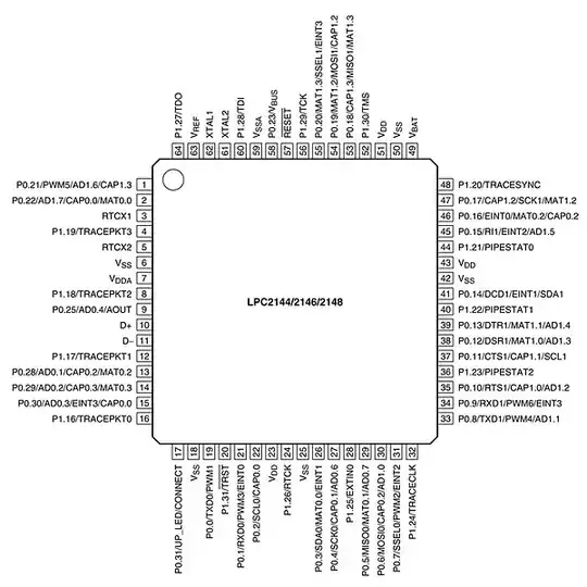
About a week back, I was handed a NXP blueboard with LPC2148 on it. Although I loved the more processing power (compared to the ATmega32s I had been working on), I found something very odd about the ARM7 based controller. If you look at the pinout here

LPC2148 pinout

you would notice that the port pins are just all over the place. In the AVR series everything is arranged cleanly with all the port pins together. Why is it not so in the LPC21xx? I cannot find any logic at all, they are not arranged by pin number or by functionality (like all the JTAG pins together). It seems like the designers just stacked the pins in a random form.

Can any body please explain the reason behind this?

Greenonline
  • 2,064
  • 7
  • 23
  • 38
Rick_2047
  • 3,897
  • 5
  • 46
  • 68
  • 3
    Good news: they *don't* do this to pester you. :-) – stevenvh Jul 12 '11 at 13:35
  • LOL! I've used an LPC2478 recently with a similar issue. I used the SDRAM peripheral which literally had pins spaced around the entire peripheral of the quad-pack. It makes keeping equal line length a nightmare. My only guess is it's easier for them to manufacture it that way. – bt2 Dec 24 '10 at 16:06
  • I am doing a lot of porting lately (atmega32 to lpc2148) and had to port code for driving an lcd to lpc. Now on atmega32 it just used two ports (its 16-bit data bus). So I figured I would just access FIO1 with two words (FIO1DIR2 etc.) but to my horror I had to solder wires instead of using the male headers as all the pins are not together. – Rick_2047 Dec 24 '10 at 16:12

7 Answers7

11

There are lots of reasons why the pinouts are the way they are.

The easiest to tackle first is the power/ground pins. Advanced chips will arrange their power/ground pins to minimize inductance and to reduce the "loop area" of signals plus the signal return path. This will improve signal quality and reduce EMI/RFI. The absolute worst thing you can do for power/grounds is what was done on the original 74xxx series parts with power on one corner and ground on the other. Xilinx has a white paper on their "sparse chevron" arrangement that is interesting. If you search on their web site they have lots of other papers and presentations talking about it with actual measured results and stuff. Other companies have done similar things without all the hype and documentation.

For MCU's where most of the pins are user configurable there really isn't a good or bad way to do the pinouts (excluding power/grounds). It's almost guaranteed that whatever they do, it'll be wrong. It is very much like us buying a dress for the wife-- no matter what, it'll be the wrong size, style, color, fit, etc. You can either compensate in software by using different GPIO pins, or by creative PCB routing, or by uncreative PCB routing (a.k.a. just adding more layers).

Another possibility is that the pinouts have been optimized for routing the PCB on minimal layers, but you're not seeing that. CPU's, for example, that require connecting to a specific chipset (or RAM) often have their pinouts designed to make that interfacing/routing easier. This is common on things like Intel CPU's w/Intel chipsets. That's about the only way you can get two 800+ ball BGA's to connect together on a 4 or 6 layer PCB filled with other power/ground planes. In these cases there are often app notes that explain how to do the routing.

And the third possibility is that it's as simple as "that's just the way it ended up". It's similar to the "whatever we do, it'll be wrong" approach, so they just do whatever was easiest or cheapest. No real magic here or mystery here. In the past there have been chips that were popular but people would complain about the pinouts-- so years later another version of the part would come out that is functionally the same but with the pins moved to facilitate PCB routing.

No matter what, in the end "it is what it is" and we just deal with it. It honestly doesn't cause too many problems, and we're so used to it that it doesn't bother us (much).
  • did a famous EE say "it is what it is" or something? There's an old school professor at my university that used to say that a lot... – NickHalden Jul 12 '11 at 17:30
  • @JGord It is a common phrase, used all over engineering, business, sports, etc. http://www.urbandictionary.com/define.php?term=It+is+what+it+Is –  Jul 12 '11 at 17:41
  • Yeah I knew that, I've just seen it with particularly high density in EE and was wondering why... – NickHalden Jul 12 '11 at 17:46
  • You can see some current shunt monitors in SOT23-5 that have their Vin+ and Vin- pins arranged differently. For example, the INA193/196. Practically the same chip, but I suppose it depends how the board is going to be routed and what's the optimal situation for pick'n'place machines. – Hans Jul 12 '11 at 19:38
7

It will certainly be a consequence of how the chip is laid out internally, combined with the fact that it is fairly rare on microcontroller applications to need blocks of consecutive IO pins to make wide buses etc., so grouping together isn't a high priority and not worth spending additional silicon area on. Of course this logic breaks down somewhat on parts with external bus interfaces, making layout, particularly with QFPs something of a nightmare, but volume users will probably be using BGAs anyway to save space - I've always thought 208QFPs look a bit ridiculous..!

mikeselectricstuff
  • 10,655
  • 33
  • 34
  • pardon the noobness, What is a BGA? – Mark Harrison Dec 25 '10 at 23:28
  • @Mark Harrison, Ball Grid Array, no pins, just an array of solder balls, typically very high density (think 121+ pins on something which would have 44 or 64 pins) but a nightmare to layout and design around. – Thomas O Dec 26 '10 at 17:04
4

IC pinouts are really determined by the layout of the circuit on the chip inside the package.

There are various considerations for IC layout designers, but it would be unlikely that external pin assignments would differ much from the die pad arrangement.

One of the considerations would be power distribution around the chip, meaning that VDD (or VCC) and ground may appear in unexpected places.

There's always a good reason for it. Believe me, IC designers don't do things arbitrarily.

pavium
  • 141
  • 2
2

It has to do with the places where a given signal comes close enough to the edge of the die to make a bonding pad for it there. That determines the order the pins will have. Sometimes a few signals could be switched, but having them all in a logical order may increase the die's size, which means extra cost.

stevenvh
  • 145,145
  • 21
  • 455
  • 667
2

IC's can have redistribution layer, which would allow to map any pin to any location, but this would just increase bare die cost by some 5-10%.

Each manufacturer choose one of the ways:

1) Design chip with fixed output pins (a bit larger die = > more expensive)

2) Have random pins (cheaper)

3) Have 1 extra layer (a bit more expensive to manufacture)

BarsMonster
  • 3,267
  • 4
  • 45
  • 79
2

The reason is that arranging the pins in a logical order is way down on the priority list of a chip company. Most designers they care about (which generally does not include hobby robotic people) will use a CAD package that has the pinout in some library, so they don't care either. So other factors, like efficient layout of the chip die, are more important.

Note that for some pins chip manufacturers do care:

  • balanced pairs (ethernet, USB) are next or close
  • the xtal connections are close (with a ground pin nearby, but not on some PICs..)
  • ground and power pins are next or close, so a decoupling cap can be added close to the pins

I remember 30 or so years ago I tried to make a single-sided Z80 computer PCB. I got most lines routed, but those silly data bus pins made it impossible.

Wouter van Ooijen
  • 48,407
  • 1
  • 63
  • 136
2

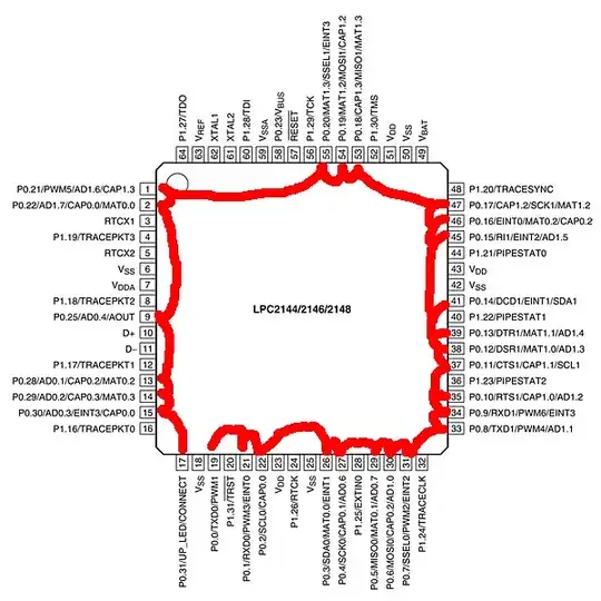
If you look carefully you can see they are in order, but not grouped together. It probably comes down to how easy the chip is to manufacture.

alt text

Thomas O
  • 31,546
  • 57
  • 182
  • 320
  • What kind of order, care to illustrate (more)? – Rick_2047 Dec 25 '10 at 17:42
  • 1
    @Rick_2047, look at the diagram, they are in sequence. – Thomas O Dec 25 '10 at 20:42
  • Seriously dude, I don't see the sequence. Your red line just shows they are all over the place, maybe I am being dense and would need some more explanation. – Rick_2047 Dec 26 '10 at 03:33
  • 1
    @Rick_2047, starting at pin #19 P0.0, pin #21 P0.1, (follow the red line, you'll see P0.x in order, except for a few special exceptions.) They are all over the place but the order isn't random. – Thomas O Dec 26 '10 at 15:00
  • Whats the use? I would need at least 8 pins to drive a data port or at least have all the peripheral pins in sequence to directly connect a connector. So the pins are random to me. – Rick_2047 Dec 26 '10 at 16:00
  • @Rick_2047 Well P0.7 through P0.14 gives you 8 or so pins fairly close to each other to drive a data port. The pins are likely in that order because it makes it cheaper to produce. – Thomas O Dec 26 '10 at 17:03
  • I cannot deny the fact that this design decision is most probably because of the manufacturing considerations. BTW, p0.7 is on the bottom row and others are on the right row. and between the other 7 pins there is p1.23 and p1.24. That doesn't look like a sequence to me. – Rick_2047 Dec 26 '10 at 18:17
  • @Rick_2047 it's in enough of a sequence for most connectors, just you need to route the traces so they are all facing the same direction. – Thomas O Dec 26 '10 at 20:41