28

In EAGLE, when you create a board from an existing schematic or incrementally add components to a linked board/schematic project, it does not overlap components in the board file.

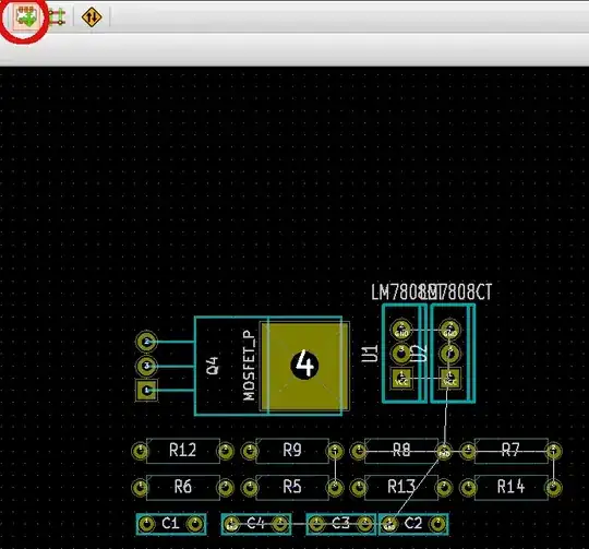
In KiCAD/Pcbnew I drew a schematic and created a board from it. Every component was placed at (0,0) which is the upper left hand corner.

I would like the components to be "exploded". That is to say non-overlapping so I can find/grab what I want instead of spending 5 minutes dragging apart 30+ footprints.

HL-SDK
  • 2,539
  • 1
  • 19
  • 26
  • 1
    I just tried 'autoplace all components'. Surely this can't be the best solution... – HL-SDK Sep 06 '13 at 15:55
  • 1
    I haven't used KiCad fro a while, but I recall that there is a "spread out the components" command somewhere, possibly involving a block move. – Peter Bennett Sep 06 '13 at 18:33
  • I find it more efficient overall to grab components by ref using the T key. – mng Sep 06 '13 at 19:46
  • 1
    I have the same problem. Where is 'autoplace all components' command ? T key method is rather good. – TMa Jul 17 '14 at 14:02

1 Answers1

39

There is a better alternative to autoplace. I think autoplace is used to minimize board space, keep things closer together for auto-routing purposes, etc. If you just want to space things out so it's easier to manually layout your board and not worry about having overlapping identical components (ie: resistors), just do the following:

  1. Open PCBNEW
  2. Import your netlist
  3. Click on the "Mode" button near the upper right of your horizontal toolbar icons right under the "File", "Edit", horizontal menus. Make sure it is depressed, and says "Mode Footprint:" when you hover the mouse over the button.
  4. Make sure you have the "Arrow" tool selected (topmost icon in the vertical list of icons on the right hand side of the screen).
  5. Right click anywhere on the board (except directly on a component), select "Glob Move and Place..." ==> "Move All Modules", and click "Yes" at the following prompt.
  6. Done, and you don't even have to create a "PCB_edges" layer. It intelligently separates the parts so they have at least a single "unit" radius (depending on your current grid resolution options) so there is no overlap with other components, as shown below.

enter image description here

Cloud
  • 820
  • 1
  • 12
  • 19
  • 10
    Note that this only works in 'default' canvas mode (press F9) – MattCochrane Dec 09 '15 at 22:38
  • 7
    It should be mentioned, that it works only in standard display mode(F9 shortcut). When openGL(F11 shortcut) mode is active this function disappears from the context menu after right-click and cannot be selected. (It gave me a head ache, before I figured it out) –  Mar 28 '16 at 11:59
  • 3
    Also worth mentioning that this doesn't work the same way if you've started to spread out components yourself - if you have started spreading components, then it'll require PCB edges to be defined. – misnomer Mar 08 '17 at 21:47