11

This question is a follow up question of the existing question: "When is using latches better than flip flops in an fpga that supports-both".

If use of latches in FPGA's is limited to rarest or rare situations, why do FPGA's have latches at all ? I mean most FPGA designs don't use it. Then why have waste FPGA hardware for such logic!

nurabha
  • 887
  • 4
  • 14
  • 29
  • What makes you think they are wasting hardware? A flip-flop is just two latches so it shouldn't be too hard to use half of a flip-flop as a latch. – Joe Hass Sep 02 '13 at 21:46
  • 2
    Xilinx's recent families (Virtex 6 and 7) only have half of their storage elements configurable as either latches or flipflops... Before that it was 100% of them. As far as I can tell none of Altera's recent FPGAs have had any latches in, and I can't recall the older ones doing so either. I think it's going away slowly! – Martin Thompson Sep 04 '13 at 12:52
  • 1
    For Xilinx's UltraScale and UltraScale+ family, the architecture guide says: "There are 16 storage elements per CLB slice. All can be configured as either edge-triggered D-type flip-flops or level-sensitive latches. The latch option is by top or bottom half of the CLB. If the latch option is selected on a storage element, all eight storage elements in that half must be either used as latches or left unused. When configured as a latch, the latch is transparent when the CLB clock input (CLK) is High." As @JoeHass said: it does not waste resources because registers are reconfigured as latches. – Daniel Wisehart Mar 31 '18 at 15:02

5 Answers5

7

I'll preface this with the caveat that I'm not that up to date on the interior workings of recent FPGA architectures. So this answer may not be appropos. depending upon whether the FPGA tools support the design flow I will discuss.

It's probably true the total volume of raw gates shipped into the market are probably latch based designs. This is because of the preponderance of microprocessor contributions to the total number of shipping transistors. So yeah, an artificial measure. In total there are relatively few people designing this way, but most processors use a scheme of:

Logic cloud -> latch (+'ve clock) -> logic cloud -> latch (-'ve clock) -> repeat semi ad-infinitum.

Which if you look at it is the canonical format for a master slave FF, but with more logic inserted between the master and the slave.

The vast majority of people, in terms of the total designs (as in number of designs)use single clock domain edge triggered. To quote Dally and Poulton (Digital Systems Engineering) "Edge-triggered timing, however, is rarely used in high-end microprocessors and system designs largely because it results in a minimum cycle time dependant upon clock skew". Use of latches driven by two-phase non-overlapping clocks results in very robust timing that is largely insensitive to skew. This adds in complexities in the design, signals from one clock domain cannot cannot be intermixed.

The other draw back is that it is rarely taught in schools.

If this was a question on high end system digital design. That would be your answer. If this applies to FPGA's - I don't know for sure but I suggest this COULD be the reason.

BTW - I'd suggest that book to anyone who is serious about advanced digital VLSI design.

"Dally, William J., and John W." Poulton. Digital Systems Engineering. Cambridge University Press.
placeholder
  • 29,982
  • 10
  • 63
  • 110
  • Could you cite an example using that clock scheme? I know ARM doesn't use it, and it causes toolchain issues (scan chain insertion etc) – pjc50 Sep 02 '13 at 21:24
  • INTEL, IBM and the reference comes from the book mentioned. – placeholder Sep 02 '13 at 21:27
  • I can confirm what rawbrawb says. In practice we used two separate clock signals and made sure that they were non-overlapping. This eliminated any possible hold time problems at the expense of distributing two clocks. The timing is tricky and I managed to shoot myself in the foot the first time. – Joe Hass Sep 02 '13 at 21:44
  • The venerable 6502 used two-phase clocking to good effect; using non-overlapping clock phases reduces the amount of circuitry required for latching, and can also ease some timing constraints. A very nice feature of split clock designs is that they can tolerate an arbitrary amount of clock skew without having to have minimum propagation delays in any latched feedback paths. The biggest problem with them is that a lot of tools aren't well-equipped to handle them. – supercat Sep 03 '13 at 00:44
6

Here's a rough list on why latches are in FPGAs:

  1. Sometimes it is the only solution. Usually when interfacing to old standards and/or equipment.
  2. Despite FF's being better some people insist on using latches. Those people also are willing to spend money on FPGAs.

And that's all I can think of. In the past 10 years, I have only used a latch once and it was for interfacing to a PowerPC where the multiplexed address/data bus required a latch to un-multiplex.

1

The main purpose of an FPGA is to implement in silicon a device which implements some desired behavior; sometimes this will require a device to perform a few functions while the main clock is shut down, or to react in limited ways to pulses which are short relative to the clock period. As a simple example, suppose one was designing a board with a discrete 74HC373 one wanted to eliminate, and had 17 spare pins on one's CPLD (assume /OE on the '373 was strapped low). Those pins should basically behave as follows:

Any time Enable is high and D0-D7 have been valid for 10ns or more, Q0-Q7 will be valid and will reflect the values on D0-D7. The Qn pins may be considered invalid, any may output anything, for the first 10ns after Enable goes high, any time Dn is invalid or changing, and for 10ns thereafter. Any of Q0-Q7 which are valid when enable goes low will hold their value until the next time Enable goes high.

Note that D0-D7 are allowed to change any any time relative to the rising edge of Enable. Thus, the rising edge of Enable can't be used as a clock. Note also that because the output of a flop won't be valid until some time after a clock edge, but Q0-Q7 are required to be valid at the moment Enable goes low if D0-D7 were valid for the preceding 10ns, the falling edge of Enable can't be used as a clock either.

While one could in theory use discrete gates to build asynchronous latching circuitry, such techniques don't work well in FPGAs. The problem is that for such circuitry to work properly, every latching feedback loop must include one or more nodes whose propagation delay is guaranteed to be greater than zero. Despite the fact real gates almost always have a positive propagation delay (in the presence of slowly-changing logic levels, a gate's output may change before its input has fully switched) it's possible for FPGA gates to behave as though they have negative propagation delay. If the wrong nodes in in a feedback loop have negative delay, the circuit may fail to operate as intended. Use of explicit latching elements which are guaranteed to have a positive feedback delay can avoid such problems.

supercat
  • 45,939
  • 2
  • 84
  • 143
1

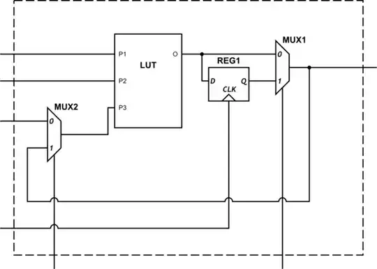
I think the confusion stems from the assertion that "Most FPGA architectures natively support both latches and flip-flops." Most of them include a flip-flop and sufficient routing that you could use the logic resources to create a circuit behaving as a latch. The schematic below shows a simplified but fairly common structure for a single logic cell in LUT-based FPGAs. By sacrificing one input for the feedback functionality using MUX2, and at the same time setting MUX1 to bypass the flipflop, you can implement a latch with two inputs. Note that these muxes are generally part of the configuration, and can't be changed during operation. Such a latch is not as predictable or fast as using the synchronous register - particularly if you only needed an asynchronous set or reset (typically only one at a time), which they tend to have. The result is that creating a latch has wasted hardware and performance. Many variations of the design exist, though, such as the Cyclone IV which can route other signals through such an unused register, but I have yet to see an FPGA architecture which provides a latch itself; if you know of one, please tell me.

schematic

simulate this circuit – Schematic created using CircuitLab

As for when to use latch logic, I can think of two scenarios. First is to detect events faster than your clock, such as to add glitch markers in a logic analyzer (the flipflop can do it at the expense of using a set/reset net). Second is to bypass a layer of registers in order to shorten a pipeline (counted in cycles) when frequency scaling goes low enough to allow deeper logic. Both of these are rather specialized situations that FPGA tools are not generally designed for. The latter actually is a bypass just like MUX1, not a latch, but is likely to cause a latch warning precisely because the tools don't expect it (and MUX1 is not controllable by logic signals), and one possible implementation uses a transparent latch.

Yann Vernier
  • 2,814
  • 17
  • 15
  • 1
    Xilinx's pre "6" series all had latches in them. "6" and "7" have 50% of their registers configurable as latches or flipflops, the rest are flipflops only. – Martin Thompson Sep 04 '13 at 12:54
  • I stand corrected! I thought I was fairly familiar with the Spartan 3 series, but indeed the text on storage elements in the CLBs does indicate support for latch mode, although symbols and truth tables are shown only for synchronous mode, even in the full slice diagram. – Yann Vernier Sep 04 '13 at 14:16
  • 2
    I wouldn't necessarily think of latches in terms of "bypassing" a layer of registers, but rather easing timing constraints so that what's required is not for each stage to complete within a clock period, but rather for the combined time of any pair of consecutive stages to complete within two clock phases (at e.g. 50MHz a device with 2ns setup/hold would require every stage to be 16ns or less; by contrast, a latch-based design might survive with a stage that took 25ns if preceding and succeeding stages only took 5ns). On the other hand, you reminded me of a point I missed in my answer: ... – supercat Sep 06 '13 at 15:17
  • 1
    If one uses conventional logic or a CPLD to compute a latch like Out=(D and E) or (Q and !E) or (D and Q), then when E is low, D can do whatever it likes without any effect (even momentary) on Q. In an FPGA, however, a LUT may interpret the expression as (D and E and Q) or (D and E and !Q) or (D and !E and Q) or (!D and !E and Q). If Q is high and E is low, a falling edge on D may cause the (D and !E and Q) term to become false before the (!D and !E and Q) becomes true, causing glitch on Q. Because of feedback, that glitch could become latched as the new state of Q. Oops. – supercat Sep 06 '13 at 15:32
0

Why FPGA's have latches when they are almost never used?

I agree that they are almost never used. From my personal experience writing FPGA designs over the last 14 years, I have yet to purposefully create a latch in one of my designs.

Having said that, I would be really disappointed if I actually needed to make one and it couldn't be implemented on the device. So that's the reason.

Also, I would say that putting in the latches is almost free in terms of hardware. If we look at something like say a Xilinx 7-series FPGA, each slice consists of four 6-input lookup tables. Each lookup table has two flip-flops at its output.

I don't have official numbers for those devices, but the flip-flop at the output might take 6-12 transistors depending on implementation. The lookup table might take nearly 1000 transistors.

So, the hardware cost of a flip-flop or latch is almost nothing compared to the total transistor count.

user4574
  • 11,816
  • 17
  • 30