How can I reverse engineer a simple through-hole board? Trying to do it by eye gets confusing because it's easy to lose track of component orientation and location while flipping the board over. Maybe there's a computer assisted technique that would make things easier?
Asked
Active
Viewed 1.2k times
33
-
8You should form the "question" part as a question (just like on Jeopardy!). Maybe something as simple as "How can I reverse engineer a simple through-hole board?" Any additional info that maybe was a stumbling block along the way will help future visitors find your question-and-answer. – JYelton Aug 28 '13 at 21:45
2 Answers
59
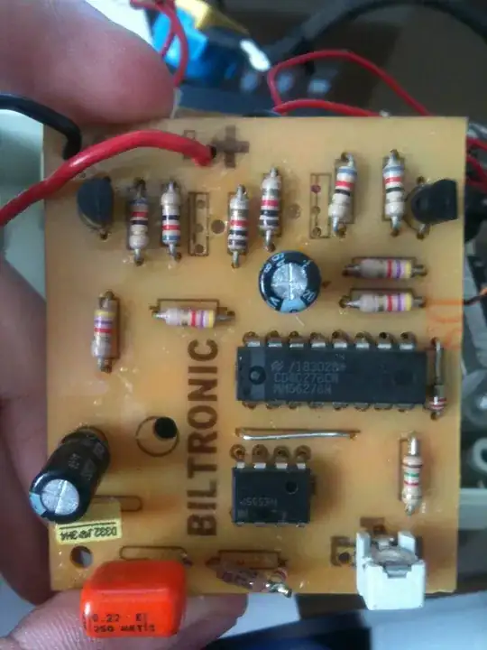
Take the best pictures of both sides of the board that you can.
You can use a scanner to scan the bottom side of the board, but not all scanners will be able to focus the top layer because of the height of the components.To this guide I used a 3MP camera of the iPhone 3GS without any special lighting or anything. You will almost always likely to have a picture taken with better equipment and conditions.
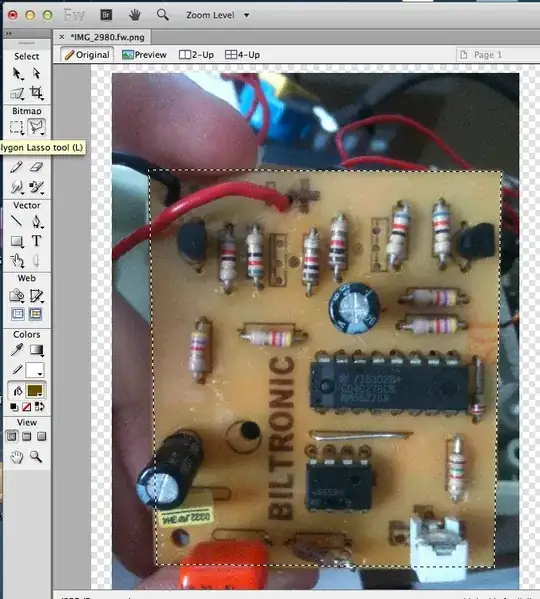
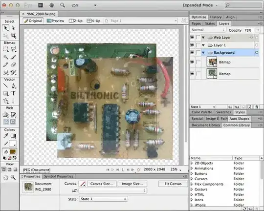
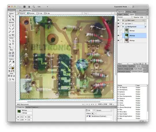
Import then to a blank canvas on your favorite editing program. I'm using Adobe Fireworks, you photoshop or almost any image editing software.
The images must be in separated layers.
Use the Polygon Lasso tool to crop the board from the rest of the picture. Do the same for the other side.
Use CMD-X to cut and then CMD-V to paste. It will lift the selection from the background. And then just delete the background. Do the same for the other side.
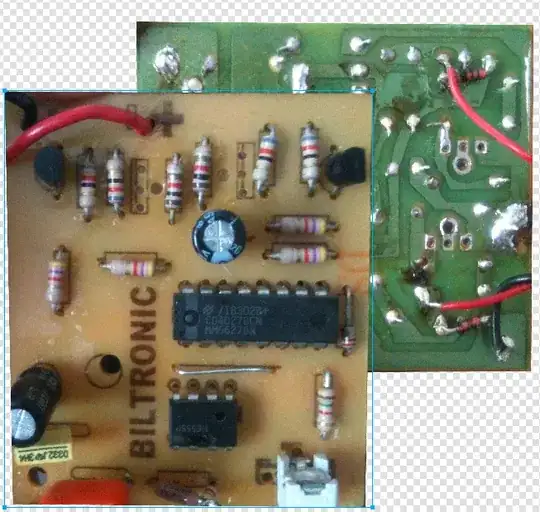
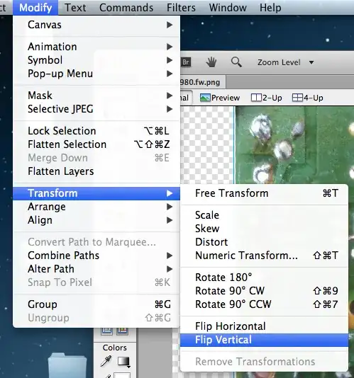
Use the Rotation CW/CCW and Flip Horizontal/Vertical to adjust the pictures to the correct position.
- You will want the bottom of the board to be mirrored, so it matches the components side.
- You will want the bottom of the board to be mirrored, so it matches the components side.
6.Decrease the opacity of the top layer down to around 50%~75% so we can se through it.
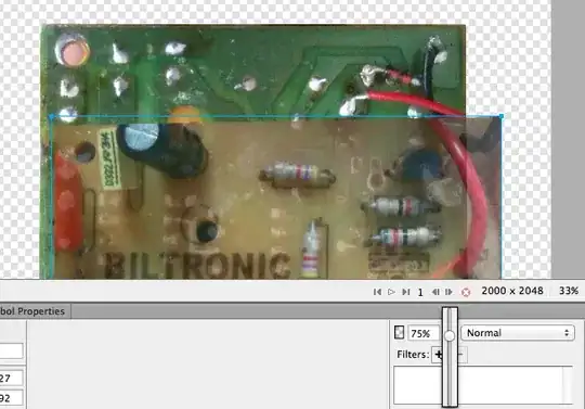
7.The 2 images are not in the same size, or angle. So we will use the Distortion tool to resize and straighten the corners of the top side so it match the bottom side.
 * Alignment is critical, so take your time, use the zoom/magnifier and check if everything is aligned. Look for the holes in the board, it is the easier way to check if the board is misaligned.
Blending
There are many methods that can be used to blend images. Not all will work on all cases.
But I will go through a few of methods that may work for the majority of people.
- The adjustments are subjective and will depend on your board color, illumination, exposure, etc... there are many variables, play around and find what values works best for you.
1. Screen Blend
- Drag the bottom side to upwards the components side (copper side's layer on top of component side's layer).
- Darken the copper layer using
Brightness/Contrastfilter and set brightness to -50 - Select the copper layer and select blend mode to
Screen/InterpolationorAverageand set to 80
2. Luminosity Blend
- Drag the bottom side to upwards the components side (copper side's layer on top of component side's layer).
- Increase the constrast of the copper layer using Levels filter, drag the pins to twords the hill.
- Select the copper layer and select blend mode to
Luminosityand set to 50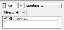
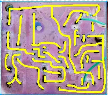
Brush + Threshold
Drag the bottom side to upwards the components side (copper side's layer on top of component side's layer).
Select the copper layer and use the Brush and draw lines connecting the solder pads/holes, you can also use the path/line tool to draw straight lines instead. Use a solid color that is not used by the solder mask. In this case the solder mask is green/yellowish, so I used blue.
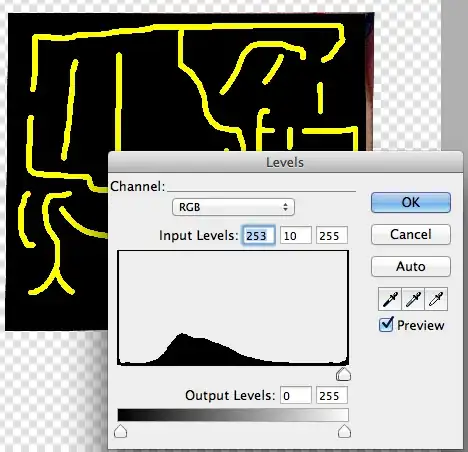
Apply a Invert filter.
Use the Levels filter or Threshold filter to extract just the solid color. Drag the left pin all the way to the right.
Apply the filter Hue/Saturation and choose the color of the track of you preference rotating the Hue.
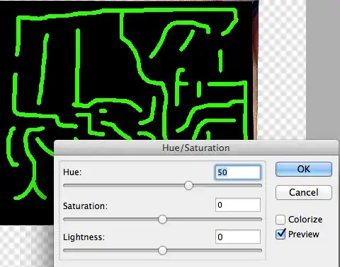
Select the copper layer and select blend mode to
Additiveand set the opacity to around 70 to adjust the intensity of the track.
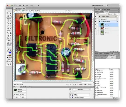
Now we are ready to write down the values, and then transfer it to a CAD Software.
Vitim.us
- 1,081
- 1
- 11
- 14
-
3+1 This looks like a really nice guide! I hope to see the rest of it. – AndrejaKo Aug 28 '13 at 21:42
-
2
-
1This is how I do it. Generally, the next useful step is to create a transparent layer where you duplicate the copper traces in opaque black. This can then be semi-transparently overlaid over the component side, so you can see the connections between the components. You can't really do this with an image of the copper side. I also use additional layers to label components. – Kaz Aug 29 '13 at 19:14
-
1You can do this for a double-sided PCB. From the images, you can trace the copper to create two transparencies for the copper layers. You can then overlay these over the component view. The real challenge would be boards with buried layers. – Kaz Aug 29 '13 at 19:16
-
2An additional trick I've employed for boards with an inner layer is to shine a very bright lamp behind the board, then take a photo from the front. The light shines through and exposes some of the inner layer, though any bottom layer copper will obscure it. From there I take the image and increase the contrast, then use the Curves tool to modify the luminosity until the internal tracks are very clear. You can usually get ~60% of the inner layer, which can be enough to guess most of the function of the circuit. – Polynomial Sep 01 '13 at 23:43
-
5
This video explains the process of reverse engineering double sided PCB's with the help of GIMP(A free software image editing tool). This same technique can be used for reversing single sided PCB's.
Here an internet router's PCB is reverse engineered. Usually internet routers are small embedded devices with an ARM processor, RAM, flash memory etc. After reversing the PCB, it is easy to find the JTAG and serial ports which will help to flash Linux into the router.
There was also a workshop which was held at CCC in 2011. Below link has the workshop details which will definitely help in reversing PCB's. Don't forget to visit all the links in the below page.
Embedded Analysis Workshop 2011
Happy Hacking!