A capacitor-based charge pump can itself not have better than 50% energy efficiency. There is a simple mathematical proof for this if you're interested.
Googling "boost converter" gives the basic schematic, which is an inductor, a switch node grounding transistor driven through PWM, a catch diode, and a filtering capacitor/output sense.
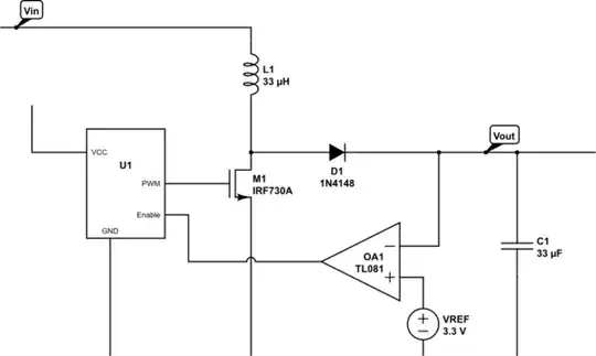
simulate this circuit – Schematic created using CircuitLab
The part numbers (Opamp, MOSFET) are whatever CircuitLab had available, not actually well-chosen parts for this circuit!
In this case, one challenging question is where the PWM would get its VCC from -- you need to bootstrap the circuit; make it run at a fixed PWM frequency before the error amplifier feedback kicks in.
Also, there will be two main losses: resistance in the inductor, and voltage drop in the diode. (There are some losses in the switch transistor and ESR of the output capacitor, too.)
The faster your switch frequency is, the smaller you can make L1 and C1, and thus get smaller losses and smaller size there, but the more switching losses you will get in M1, and the harder the circuit board layout becomes.
You can also use a synchronous rectifier setup (second MOSFET instead of D1) to reduce D1 voltage drop losses, which will be huge in this circuit (almost 20% on its own!)
Given that the input is 0.5V, and you want output 3.3V/60mA, and the D1 drop is 0.7V, then you need a 8:1 voltage gain, so at least 560 mA through L1. L1 will have a resistive voltage drop, so you're going to want to look for 12:1 or better gain. (3.3V+0.7V)/12 = 0.333V, so the allowable drop over L1 is 0.167V, so Ohms law says maximum resistance of L1 is 0.298 Ohms. Yet another source of loss -- getting to 80% efficiency is going to be really hard!