4

I operate a N-MOSFET (2N7000) in a simulator in the linear region very close to \$V_{DS}=0\$. In fact \$V_{DS}\$ is between \$-50nV\$ and \$+50nV\$.

schematic

In the simulator the output seems linear, but is this in reality happening? What happens if \$V_{DS}\$ goes a few tens of \$nV\$ below \$0V\$ ?

\$V_{GS}=5V\$ constant (on state)

Phil Frost
  • 56,804
  • 17
  • 141
  • 262
Chris
  • 554
  • 6
  • 13

2 Answers2

4

If by linear you mean drain current and voltage are linearly related, then:

MOSFET modes of operation

You are in the linear operation region, upper right. Between the drain and source is an inversion layer, and this looks mostly like a resistor.

If \$V_{DS}\$ goes negative, then the current will go the other way. Since the gate voltage is (relatively) very high, there's nothing in the channel to make it significantly asymmetrical.

However, there is another effect in play. Notice that the drain in an N region, sitting in a P substrate. Smells like an NP junction diode. In fact, this is the infamous body diode. At \$V_{DS} = -50nV\$, this diode won't be conducting much. However, as \$V_{DS}\$ becomes more negative, the effect of this diode will become more significant, and the drain current-voltage relationship will become progressively less linear. That depletion region in the image will become progressively thinner, until it's not there at all, and you have forward-biased the diode completely, and \$V_{DS}\$ will be clamped at about \$-0.65V\$.

Phil Frost
  • 56,804
  • 17
  • 141
  • 262
  • I'd add in that most simulators in this linear trans-linear region handle it nicely. But I'd stay far away from the forward biasing the S-D-Channel/Bulk connections as the "leakage current" will dominate, so at most - 100 mV or higher. One word of caution, not all SPICE decks incorporate the S/D connections and leakage models for them so might ge really good results that don't work in real life. There are a whole class of circuits called Translinear circuits that use this effect to extend operation range. – placeholder Aug 17 '13 at 15:40
  • Reading in the provided datasheet I see that the transistor in question is DMOS. This answer is almost completely irrelevant to DMOS structure of the transistor and, therefore, wrong. – Vasiliy Aug 17 '13 at 20:22
  • @VasiliyZukanov I'd believe you, if you explained why, but your answer just looks like a tirade on how everyone else is wrong without any explanation of your own. I don't see any real arguments contrary to what I've said. – Phil Frost Aug 17 '13 at 22:05
  • Do you KNOW what a DMOS is? It is a CMOS structure with an Extended drain region to allow a voltage drop across the drain. Often (i.e. the DMOS that I designed - following industry standards) has the drain structure go under active and then back into a normal CMOS structure. – placeholder Aug 17 '13 at 23:06
  • @rawbrawb perhaps you should write an answer. – Phil Frost Aug 18 '13 at 01:13
  • @PhilFrost, this question is not usual and not simple and concerns one particular transistor. You tried to justify your answer using the most basic model of MOSFET, which is not appropriate for this case.There is nothing to explain - you can't predict the behavior of the device if you're using the wrong model. – Vasiliy Aug 18 '13 at 07:34
  • @rawbrawb, are you sure that the structure you described is DMOS and not DEMOS? In general, are you sure that all DMOS transistors have the same topology? I added another section to my answer - please see it. I hope this will explain you why I insist that no theoretical answer can be provided unless you can obtain a silicon level schematic of this DMOS – Vasiliy Aug 18 '13 at 07:47
  • @VasiliyZukanov yes. The basic concept is to provide lateral voltage stand off with an extended structure. Read this link for an explanation in the DEMOS section. http://www.vlsi.itu.edu.tr/ituvlsi/webs/courses/undergraduate/ele413/student-groups-1/20102011/students/murat-dogu/homework-i/power-mos-devices-ldmos-dmos-demos-dddmos – placeholder Aug 18 '13 at 15:01
  • @rawbrawb, am I understand correctly that you described DEMOS transistor when trying to explain what DMOS is? If it is the case, then I believe my point is proven. P.S. No need to argue that DEMOS is kind of DMOS. – Vasiliy Aug 18 '13 at 15:18
0

I think that the simulation can't provide you with the answer to this questions because basic transistors models are developed to be accurate in the forward regions of operations.

The only correct answer may be obtained from building a test circuit and measuring the response of the actual transistor.

In order to give you even approximate theoretical answer (with high degree of confidence), we will need to see the actual internal implementation of the transistor (silicon schematics) - not all transistors are built in the same way, therefore there is no general answer can be given. Manufacturers tend to keep the manufacturing technologies secret, therefore your chances to get a reliable theoretical answer are very low.

I say buy few transistors and go to a lab.

EDIT:

Few folks in the comments suggested that this answer is incorrect because there are no low level Spice models for this transistor. Here are two:

However, even obtaining Bsim3 model for this device does not necessarily means that the simulation will give correct results. At least two reasons for this:

  • There is no way to know how accurate your model is
  • Even if the model is accurate for the forward biased transistor, these models (to my knowledge) are not required to be accurate for reverse biased devices. This means that there is no one who can give you any guarantees as to the accuracy of the results in the conditions you mentioned.

Have a look at this reference. These guys tried to model trench power MOSFET with custom tailored Bsim3 model. While the accuracy in forward region of operation is good, it is not perfect. And still, no one gives any guarantees as to the accuracy of reverse bias modeling. They also note that there are additional difficulties in applying this model to other topologies of power MOSFETs.

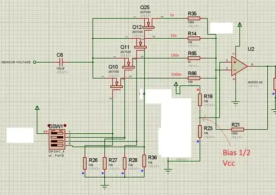
Now, the transistor in question is DMOS, therefore any analysis performed on the model of simplest "logic" transistor will be inherently wrong.

EDIT2:

Why I'm that sure that no theoretical answer can be given unless we see the silicon schematic of this particular transistor? Well, the only hint Fairchild provided in the datasheet is that this transistor is of DMOS type. This could be helpfull in some way if the term DMOS was unambiguous, but it is not the case. There are many completely different topologies which called DMOS by different groups of engineers. Few examples:

These two references show at least three different topologies which may be reffered as DMOS, and there are more.

Anyone who is trying to explain how the transisto in question works without seeing the silicon implementation is just speculating (unless he works for Fairchild, in which case he discloses trade secrets :))

Vasiliy
  • 7,323
  • 2
  • 21
  • 38
  • The core algorithms and models of SPICE can handle this fine. AS long as you account for the parasitic diodes and their current shunting (not all models incorporate them) the simulations match with real world results. See comments in Phil Frosts answer. – placeholder Aug 17 '13 at 15:43
  • @rawbrawb, I disagree completely. You do not know which model does OP use for this simulation. This could be level1, 2, 3, bsimX or any other and the results would be completely different for these models. In order to account for parasitic diodes one MUST know the physical implementation of the transistor, which is rarely the case. – Vasiliy Aug 17 '13 at 15:46
  • I challenge you to find a single example of available modelling tools that uses SPICE models BELOW level 49. Even if the code does exist, new users aren't going to be recompiling and reusing it. Knowledgeable people know better than to use flawed code. – placeholder Aug 17 '13 at 15:56
  • Clearly there are highly detailed models for the almost-vintage 2n7000. In fact I can't even find anything for LTSpice 4 or pSpice, which does not represent a detailed model down to body diode conduction level. That tells me this answer is either ignorant or plain irrelevant. – Anindo Ghosh Aug 17 '13 at 16:41
  • @rawbrawb, I don't know about tools, but I found plenty of low level models on the web. See the edit to the answer for additional info. – Vasiliy Aug 17 '13 at 20:10
  • @AnindoGhosh, a quick search in google found many low level models. See the edited answer. Furthermore, my point is that even the most sophisticated models are not required (to my best knowledge) to be accurate in reverse operating conditions. I'll be glad to read any reference showing to what degree do Spice models fit the experimental data for reversely biased transistors. – Vasiliy Aug 17 '13 at 20:13
  • @AnindoGhosh, what do you mean by "down to body diode"? What is the meaning of this crucially important body diode in DMOS transistor? How can you know which topology did Fairchild use in manufacturing of this transistor? – Vasiliy Aug 17 '13 at 20:33
  • @VasiliyZukanov "down to body diode *conduction level*". Your edits and comments seem to be deliberately misunderstanding feedback. Not a game I want to play any more. – Anindo Ghosh Aug 18 '13 at 02:38
  • @AnindoGhosh, no game, really. I respect your opinion and all I wanted to show you is that the term "body diode" is ambiguous when referring to DMOSs in general. The only way to give any reliable theoretical answer to this question is to see the silicon implementation of the device OP asked about. Any other approach is just a speculation, which is not an appropriate approach for answering such an interesting question. See additional edit to my answer to understand why I insist on this. – Vasiliy Aug 18 '13 at 07:59