6

I have a pcb with a SPI bus with several sensors that have to be connected to this bus. Since 90 degree traces are not recommended in a proper PCB design I ask myself how to connect so many sensors without using sharp turns and perpendicular traces?

I am thinking about making triangles to smooth the connections, but I wanted to ask it here before if there is a recommended way for doing it.

PS: Maybe someone will say that SPI speeds shouldn't have trouble with this, but still it's a valid question for learning purposes.

EDIT:

Since an image speaks more than 1000 words...

That's the problem I am presenting: "how to eliminate 90 degrees traces in a bus connection?" (even if in this particular SPI case I won't have a problem, it still triggers my curiosity)

Signal Bus Line

mFeinstein
  • 4,293
  • 11
  • 45
  • 84

4 Answers4

15

Quick answer: 90 deg bends are not an issue for most things. I don't do them purely from as aesthetic point of view. It only becomes an issue somewhere higher than about 500 MHz, but even then it's questionable.

There are three reasons to not do 90 deg bends: It causes an impedance mismatch, and thus messes up signal integrity. The sharp corners get rounded off during the PCB etching process and can weaken the trace. The bends cause some sort of reflection, unrelated to the impedance mismatch.

It has been shown that the impedance mismatch issue is a non-issue. There are many sources for this, but the best one is in the book "High Speed Digital Design: a handbook of black magic".

Weakening of the trace can be significant, particularly if your trace widths are on the edge of what the PCB shop can make. But I personally have never had issues with this, and don't know of anyone who has had an issue. So I can't say that it is a serious issue.

As for the wave of the signal bouncing off of the flat face of the trace, I am not sure if that is real or an EE urban legend. What I do know is that you need super fast edge rates to even bother thinking about this. Almost everyone here on EE.SE can ignore this.

What is more important than the shape of the trace is the "holy trinity of signal integrity": Trace Impedance, Signal Return Path, and Signal Termination. Get these right and almost everything else doesn't matter. Also, you should do this for almost all signals in a digital design, regardless of frequency!

Update: I'm adding stuff to directly address the schematic-like things the OP added to the question.

For starters, don't worry about the 90 deg thing. Not an issue.

Next, consider that SPI has two types of signals: One driver feeding one receiver, and one driver feeding multiple receivers. MISO and MOSI are examples of one driver feeding one receiver. SCLK, and CS are the signals the feed multiple receivers. Understanding this distinction is super important, since each type of signal will require different PCB layout techniques.

I'm going to describe how I deal with these signals. I rarely do 2 layer PCB's, most are 6 to 8 layers. What this means is that all of my PCB's have ground and power planes. This is super important, because properly handling signal integrity is almost impossible in a 2 layer board. Also, this is a big topic so I cannot write about everything. Where appropriate, I will give you terms to Google.

We'll start with the one driver feeding one receiver (MISO or MOSI), since this is the easiest. For these, I use a type of signal termination called "Source Serial Termination", or sometimes just called source termination. At the driver, in series with the signal, is a simple resistor of around 25 to 75 ohms. The exact value of this resistor has been calculated to match the impedance of the trace minus the source impedance of the driver. So if my trace is 50 ohms, and the driver has a 20 ohm output impedance then my resistor will be 30 ohms, +/- 10%.

The trace impedance can be calculated using the various formulas for "stripline" and "microstrip" traces (Google those). I normally target a 50 ohm trace impedance, and vary the trace width to get that. The signal layer of the PCB needs to be really close to the plane, otherwise the trace needs to be unrealistically wide. I construct my PCB Stackup (how the layers of the PCB are made up) to assure that the space between the signal layers and the plane layers is appropriate.

One reason why a 2-layer PCB is almost impossible to do this with is because the space between one layer and the next is super large and also you basically have no control over it. The other reason is that you rarely have a SOLID plane under your signal traces.

Another thing is that you rarely know the output impedance of your driver. Usually I just guess at about 10 ohms. Other times I'll just put a 50 ohm resistor there and expect to tweak the value once the PCB is made. I use a fast o-scope with proper ground connections and probing at the receiver when looking at the signal.

So, back to our signal... The resistor is placed as close to the driver as is reasonable. Then I route the signal directly to the receiver. Along the way I make sure the trace width is correct for the impedance I want. Next, I pay attention to the signal return path. Google "Signal Return Path" and "Loop Area". It is important that the signal return path say directly under the signal trace, and proper use of decoupling/bypass caps are used when the return path has to jump from the power plane to the ground plane or vice versa.

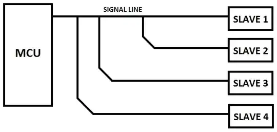
Now for the one driver-multiple receiver signals. These are much harder. The most important thing is that the signal must be daisy chained. In your case, the output of the MCU must go to slave 1, then from slave 1 to slave 2, then from slave 2 to slave 3. You cannot do it how you drew it in your diagram, where it goes out from the MCU and then branches out to all of the slaves. The second most important thing is that your signal termination must be at the very end of the line, after the last slave, and not at the MCU like the previous example.

(Note for the pedantic among us: What I said in the previous paragraph is not strictly true, *BUT... The single driver-single receiver has a difficulty of a 2 on a 1 to 10 scale. The daisy-chaining single driver-multiple receiver signal is about a 3 or 4. Doing a star routing, which is what you drew in your question, is about a 9 on our 1-10 scale. You can do it, but you'll regret it.)

For these signals, you have more options for your signal termination. The ideal termination would be a resistor from your signal to a power rail that is exactly half of your signal level. For example, if your signal goes from 0 to 3.3v then your resistor would go to a power rail that is 3.3/2, or 1.65 volts. The value of the resistor would equal the trace impedance (same microstrip/stripline formula as before). The regulator on this power rail needs to be a special type that is made for signal termination-- because it has to sink as well as source power (there are exceptions to this).

Of course, not everyone has a 1.65v rail just lying around, so there are options. If it's not a super critical signal, I might use a rail that is down to 1.5v, or as high as 1.8v. Or I might use two resistors, one to GND and one to +3.3v, instead of a single resistor (Google "signal termination" for the formulas). Or I might use a single resistor plus a cap in series, called AC termination.

The bad thing about using two resistors, like a voltage divider, as termination is that it can use up a lot of current. The good thing about AC termination is that it uses very little current. But many people get AC termination very wrong. AC termination only works for signals that have a 50% duty cycle and are always wiggling. Signals that do this are called clocks. :) But the SPI Clock does not apply, because it can be turned off and so it does not always wiggle. The other mistake that people make is that the cap is very small. Sometimes only a dozen pF. That cap should be at least 0.01 uF, and I often use 0.1 uF. A small cap here is a sure sign of someone not knowing what they are doing.

Anyway, so daisy chain these signals and put proper termination at the very end of the chain.

I have just barely scratched the surface of this issue, and it might take years before you fully understand the topic. There is a lot of info on the 'net about this, but unfortunately there is a huge amount of mis-information on the net as well. Beware.

I will end this with some things that should raise red flags. If you see any of this in some schematics, or in what someone writes, you need to run away: Just because the frequency of a clock, or the data rate, is slow does not mean it doesn't need signal termination. A 100 KHz digital signal usually requires proper signal integrity (SI) stuff just as much as a 100 MHz signal. Anytime someone add stuff to the circuit to "slow down the edges", that is a sure sign he/she doesn't have a clue. Anytime a cap is added directly to a signal, that's bad (with the exception of EMI filtering at connectors). As I mentioned before, using a pF-sized caps on AC termination. And finally, not verifying the SI with a good scope and proper probing can be fatal to your design.

  • "The bends cause some sort of reflection, unrelated to the impedance mismatch." Care to elaborate? – Phil Frost Aug 13 '13 at 17:32
  • 1
    Without mitring, a 90 degree bend has a small extra capacitance compared to a straight trace. Whether this is related or unrelated to impedance mismatch is a semantic question rather than a technical one. As for weakening the trace, are you thinking of the possibility of etchant trapping in the *inner* corner rather than rounding of the outer corner? Rounding the outer corner would actually improve the capacitance issue. (That said, I agree that below 500 MHz you probably don't need to worry about it) – The Photon Aug 13 '13 at 17:43
  • 1
    @PhilFrost As I said, this might fall under the category of urban legend. As the story goes, the wave of the signal hits the 90-degree "wall" and reflects back to the driver. If it is at a 45 deg angle it will reflect off the wall at the angle, more toward the receiver. My gut instinct is that this is pure BS, but I am not super good at the nuances of RF so I'm not prepared to commit to that. –  Aug 13 '13 at 18:13
  • @ThePhoton I was specifically thinking of rounding off of the OUTSIDE corner. This would make the trace thinner, and thus weaker. I didn't mention the whole acid trap thing, but if this is also an issue then you get a double-whammy and the trace is extra thin. It is just another thing to consider if you're making a board with already fine traces (at the edge of what the PCB shop can do). As a point of reference, I recently had a PCB with some small square pads. The corners of the pads were rounded off with a 3 mil radius. I would not do 4 mil thick traces with this PCB shop. –  Aug 13 '13 at 18:20
  • @DavidKessner I wouldn't put it in your answer unless you can back it up with references. This is how legends, misconceptions, and misinformation propagate. – Phil Frost Aug 13 '13 at 18:22
  • 2
    @PhilFrost I had to mention it because it is something that I commonly hear, and the OP will hear it. I said the important part, which is that it might be urban legend and that it can safely be ignored for this situation. If you have information that would clear that up, then post it. Otherwise, I am satisfied with my answer as is. –  Aug 13 '13 at 18:30
  • 1
    I would worry more about the acid trap issue than the corner rounding. The main reason for the excess capacitance at the corner is that the trace is effectively wider as it goes throug a 90 degree corner, by a factor of sqrt(2). Rounding off this corner (up to a point) will probably just make the corner closer to being the same width as the straight parts of the trace. – The Photon Aug 13 '13 at 18:30
  • @ThePhoton Yeah, as I said, I haven't had it be an issue. I also have never had issues with acid traps. Just something to be aware of, but there is no reason for people to get paranoid about them. In my opinion. –  Aug 13 '13 at 18:34
  • I have heard about signal reflections in several different places, I don't think it's a legend, just too much unlikely to happen in most frequency regular people deal with...but not the black side wizards – mFeinstein Aug 13 '13 at 19:53
  • @DavidKessner could you please elaborate more on the image I presented now? Even if in this case, in this frequency it wont be an issue, I am still curious about how to do a proper bus routing in high frequencies. – mFeinstein Aug 15 '13 at 05:31
  • @mFeinstein Elaborated the answer. –  Aug 15 '13 at 14:16
  • @DavidKessner great answer! which book do you recommend on SI? High-Speed Digital System Design: A Handbook of Interconnect Theory and Design Practices or High Speed Digital Design: A Handbook of Black Magic or High Speed Signal Propagation: Advanced Black Magic or Signal and Power Integrity - Simplified (2nd Edition) or Signal Integrity - Simplified or something else? – mFeinstein Aug 17 '13 at 23:25
8

As you guessed, at 20 MHz you will have no problem designing with 90 degree bends. You probably don't even need to worry about setting up your trace geometry to obtain a controlled-impedance microstrip or stripline.

If you were designing at 50 MHz or higher, you would probably want to design with a trace geometry that gives a roughly controlled characteristic impedance (except for very short traces).

Above 100 or 200 MHz (depending on trace length and your application requirements), you probably want to specify to your board fab that they must control trace impedance.

For designs at at 200 MHz to 1 GHz you you might start worrying about avoiding 90 degree bends. Then you could simply use two 45 degree bends, with maybe 20-100 mil of trace between them, to turn your trace by 90 degrees.

If you were designing above 1 GHz you might even want to avoid 45 degree bends, then you would use smooth arcs to turn the trace. You'd also do everything you can to avoid vias.

Of course the frequency bands I give for these different techniques are rough estimates. Some designs at 1 GHz might have exceptional signal itegrity requirements and so you'd use arcs. Some designs at 500 MHz might have relaxed requirements and allow you to use 90 degree bends, etc.

Engineering is as much about keeping cost down and getting a job done on time as it is about optimizing a design to the point of perfection. If your design doesn't require something fancier, 90 degree bends will probably let you reduce board area and multi-layer Manhattan routing will get the layout done quicker, so messing around with arcs or optimizing to avoid vias would be poor engineering. 45 degree bends, frankly, aren't that much more pain to design, but they do probably cause some increase in required board area.

Edit

(responding to the update to the question)

Apparently what you meant by a "bus" was a line with connections to multiple devices, rather than several lines routed together from one place to another, and you're concerned about places where the line branches.

In this case, on a single routing layer, a 90 degree connection is the best you can do. What you want to avoid is acute angles in the copper edges. These (at least historically) could cause etchant to build up during manufacturing and cause broken traces. As alluded to in comments on David's answer, it's rare to have a problem with this with an up-to-date high-quality shop nowadays. But if your trace joins at anything other than 90 degrees, there will be an acute angle on one side or the other and you manufacturing shop will probably still appreciate if you avoid that.

What you really want to avoid here is long stubs off of the line. Long meaning more than 1/10 (or so) of the wavelength associated with the highest frequency of interest.

Asusming the signal source is in the MCU and the receivers are in the slave blocks, its preferrable to route, for example, from the MCU block to Slave 1, then from slave 1 to slave 2, from slave 2 to slave 3, etc. With as short a stub as possible branching off to each of those devices. If you were working with controlled impedance, you'd place the termination at the end of the whole chain, after the line passes by all the slaves.

Of course if the signal source is in the slave device, being sent to the MCU, then the slaves in the middle of the chain would still be driving into a branched line. There isn't as far as I know any great solution for this. It puts a practical limit on the frequency of communication in a bidirectional multidrop bus like this. Although you can look at things like DDR3 layout recommendations to see how far this can be pushed. For higher frequencies, you'll find that point-to-point rather than multidrop topologies become much more common.

The Photon
  • 126,425
  • 3
  • 159
  • 304
  • I always do 45 degrees turns, but for single traces...my question is more for a bus, because in the bus there will be a straight line and several 90 degree connections "grabbing" this trace signal so I am wondering how to avoid the 90 degrees connections in the bus. Maybe it's not clear so I might add a picture later when I get home. – mFeinstein Aug 13 '13 at 19:27
  • What's Manhattan routing? – m.Alin Aug 14 '13 at 11:31
  • @m.Alin, Since I don't find a Wikipedia article on it I can link to, or another question about it on EE.SE, it would make a good question for the site. – The Photon Aug 14 '13 at 15:54
  • @m.Alin, most of the time someone says "Manhattan" it means a grid, just like Manhattan's streets and city layout...like Manhattan Distance, so I assume it's the same in routing, since a ground grid is always desirable as a low impedance return path....but place it as a question anyways, its good to have it documented – mFeinstein Aug 15 '13 at 05:34
  • @mFeinstein, Like christenson says in his answer, before you start worrying about stub lengths and 90 degree bends, you should be designing with a full, unbroken ground plane, not a ground grid. – The Photon Aug 15 '13 at 15:31
  • @ThePhoton, sorry I didn't made my self clear...I did not mean to say that a grid is what people should look after...but that usually the word "Manhattan" is associated with a grid design... and yes as you said usign a plane is always better, but since most planes will have holes so signals can flow through layers, they tend to look as a fine grid as integration level goes higher...the plane is actually the grid concept of multiple return paths taken to infinity no questions about that... – mFeinstein Aug 15 '13 at 15:38
  • @mFeinstein , The Photon I just posted [a question about Manhattan routing](http://electronics.stackexchange.com/questions/79145/what-is-manhattan-routing).. – m.Alin Aug 16 '13 at 08:37
2

The other answers ASSUME something I think the hobbyist original poster doesn't know:

The single most important thing to do is to place the traces over a GROUND PLANE. It's an SPI bus, which probably runs somewhere under 10MHz, so a little termination would really be icing on the cake.

In practice, I might place 50 ohms in series with the driving pins to achieve some damping. He or she really isn't working at a high enough frequency for the other techniques to matter.

  • thanks @christenson, but I am aware of inductance minimization about a proper use of a ground plane, avoid crossing slots and etc. What NO ONE answered is about the REAL question, about the geometry of the traces in a bus, I made it clear its not a question just about my particular case. And it's a 'he' not a 'she', and I am not a hobbyist, but an engineering student, so I am sorry, but there are lots of assumptions in there... – mFeinstein Aug 15 '13 at 05:28
1

A 20MHz clock (yours may be faster) has a wavelength of 15metres and to avoid the problem of termination resistors, the maximum distance for transmission over a PCB to other SPI devices should be significantly less than 15m and some folk will go for one-twentieth of the wavelength.

So, at a distance of 75cm (still a very large PCB) you should be OK with "normal" routing techniques i.e. conventional vias and 90 degree angles when you swap layers etc..

If you are using a +100MHz clock (I've heard that some do) then you ought to be thinking about using proper high-speed routing techniques and also keeping clock and data lengths equi-distant.

Caviat

Remember that the master clock not only clocks data to the slave devices (hopefully arriving in sync for each one) but it also clocks back the replies from slaves and this can never be in-sync so this is another consideration on maximum distances on PCBs. Good tracking won't help this problem.

Andy aka
  • 434,556
  • 28
  • 351
  • 777
  • 3
    A 20 MHz clock would have much higher frequency edges, right? – m.Alin Aug 13 '13 at 12:16
  • Why the replies can't be in sync? – mFeinstein Aug 13 '13 at 12:59
  • And as I said: "PS: Maybe someone will say that SPI speeds shouldn't have trouble with this, but still it's a valid question for learning purposes." So I meant it as a question not only for my particular problem, but more as a curiosity. But thanks for the reply anyways. – mFeinstein Aug 13 '13 at 13:01
  • "Avoid the problem of termination resistors" is opening a can of worms. Where I work we pay attention to signal termination on traces of more than 2 inches, even when running clocks as low as 50 KHz. We do this because it matters, and we've learned our lessons the hard way. And signal termination isn't that difficult after all. –  Aug 13 '13 at 17:14
  • @DavidKessner On an SPI bus what would you do if it were several inches to the furthest chip. I know I'd probably put 10pF in series with 30 to 100 ohms as a precaution i.e. not a full logic level killer but enough to prevent any "nasties". Maybe it might make a decent question? – Andy aka Aug 13 '13 at 18:20
  • @Andyaka On signals with exactly one receiver, I would put a source termination resistor (25-75 ohm resistor at the driver output). On signals with more than one receiver, I would daisy-chain the receivers and put a single resistor to a "termination voltage power rail", which is exactly half of your VCC rail (so, 1.65V if VCC=3.3). Anytime you see a small cap (less than 0.01 uF) in series with a termination resistor, and/or the signal is not a 50% duty cycle clock then that is a sure sign of someone not knowing what they are doing! Seriously! Ask me in chat if you want more about that. –  Aug 13 '13 at 18:26
  • @DavidKessner OK I see what you mean and I didn't make it very clear - I'd put the series (C and R) in parallel across data line to ground!! Maybe I'm still being stupid! It has been known LOL – Andy aka Aug 13 '13 at 18:56
  • Don't go private haha I am learning by your discussions...I am new in signal integrity and its so many things to give you invisible problems that it makes me insecure as hell haha – mFeinstein Aug 13 '13 at 19:17
  • @mFeinstein I wasn't meaning a private chat. Public is fine. It is just that this discussion could easily go off topic or discus things that are better done in a chat rather than here. Comments to answers are not intended for extended discussions. –  Aug 13 '13 at 19:22
  • Yes you are right, I just wanted to see it documented somewhere – mFeinstein Aug 13 '13 at 19:29