3

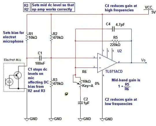
I have this circuit I built long ago to amplify 2mV signal from speaker and phase shift it by 2.5V.

Now the question is, what does C2, C4, R5, and R6 exactly do?

http://postimg.org/image/u4m4kvr99/4322863b/

JYelton
  • 32,302
  • 33
  • 134
  • 249
gargoor
  • 47
  • 2

3 Answers3

4

R5 and R6 set the gain of the circuit.

C4 technically changes the frequency response, giving it a LOWER gain at higher frequencies, but the value of the cap implies that it's just there to add some stability to the circuit and won't effect the audio frequency response too much.

C2 also changes the frequency response of the circuit-- reducing the gain at low frequencies. Basically, cutting off the bass frequencies. I am assuming (I have not calculated) that this will cut off frequencies below about 200 or 300 Hz.

Technically, C2 is doing the same function (High Pass Filtering) as C1+R2+R3. Odds are high that you could remove C2 (short it out) and have a circuit that works just fine.

UPDATE: I should also mention that this circuit is missing a DC blocking cap on the output. This is normally done, especially when the opamp is ran off of a single supply rail.

  • C4 reduces the gain at higher frequencies (which I'm sure you meant) probably for stability as you mention. – Oli Glaser Aug 08 '13 at 18:34
  • David Kessner . So you are saying that C4 and R5||R6 can are there to define the cut off frequency – gargoor Aug 08 '13 at 18:56
  • So David Kessner , Oil Glaser this what you mean Gents : fc = 1 / 2*pi*(R6||R5)*C4 – gargoor Aug 08 '13 at 18:58
  • @OliGlaser Yes, lower gain at higher frequencies. Good catch. –  Aug 08 '13 at 19:16
  • gargoor R5+R6 define the overall gain. R2+R3 define the DC bias point. These are the first values that are picked. After that, you choose the value for C1 and C2 to set the frequency response. Of course they are all inter-related, but in this circuit it's R's before C's. @Kaz's description of how C2 operates is better than mine, but we approach things from slightly different angles. I completely forgot to cover the whole DC Bias thing with respect to C2. –  Aug 08 '13 at 19:20
  • @David Kessner y I added R2 and R3,for the reason that i want the signal to operate on 2.5V so I can feed it to Arduino Uno bcz the MCU takes in 0v to 5v , that's why i didnt add an output cap . Thanks for bringing my attention to R2+R3+C1 form a LPF. C2 is added so to block any DC common ground signal so it Doesnt get amplified and thus also affect the power supply. I cant get the idea of you saying it has low gain at low frequencies. There is one thing i would like to change , I want the Cutoff frequency to be at 4K. btw what type of amp is this ? its not integrator opamp right ? – gargoor Aug 12 '13 at 15:13
  • @gargoor I have no idea what this type of amp is called. I never really referred to it by any special name. To me it's just a mic preamp, or a high pass filter with gain, or whatever. There are so many different circuits that use opamps that it is often not worth naming them all. –  Aug 12 '13 at 15:19
4

C4 reduces closed-loop gain at high frequencies. It is a form of dominant pole compensation to fend off the risk of amplifier instability. It shouldn't be necessary with internally compensated op-amps, but it's good to leave a spot on the circuit board for it.

As for C2, primarily it is needed for proper biasing. If R6 were connected directly to ground, the amplifier would have a large DC offset at the output. The feedback cannot be referenced to ground because the amplifier is based around the 2.5V operating point. C2 provides an "AC ground" for the feedback loop, without coupling it to the 0V DC ground. The presence of C2 has the side effect that the amplifier has only unity gain at DC: bass is rolled off, in other words.

Rheostat R6 controls the gain, which, ignoring frequency effects, is basically \$1 + R_5/R_6\$. The smaller the resistance that is dialed in on R6, the bigger the gain. The particular wiring of a potentiometer to serve as a rheostat shown in the schematic is a good method, because if the wiper of the potentiometer happens to make an intermittent contact, the resistance of the part will not go above that of its resistive element. The circuit has a minimum gain, when R6 is maximum, with no upper bound on the gain: when R6 is turned toward zero, the gain increases rapidly toward a large value. The circuit designer wanted the user to be able to get large amounts of gain from a single op-amp stage.

By the way, since C2 blocks DC, it also ensures that R6 operates quietly. When significant DC flows through potentiometers, they can create a scratchy sound when operated.

This circuit has a bit of a flaw: the designer neglected to capacitively bypass the voltage divider formed by R2 and R3. That is to say, R3 should be paralleled with a capacitor to reduce power supply ripple, which will appear as a signal at the node between R2 and R3. Thus the design relies on VCC being well regulated.

Kaz
  • 19,838
  • 1
  • 39
  • 82
  • This is interesting, but I'm curious how the op-amp is performing with a virtual ground for the feedback loop when there is no negative supply for the op-amp. – akohlsmith Aug 13 '13 at 18:27
3

enter image description here

Hope I haven't missed anything. Well possibly I did - David Kessner reminded me that answers sometimes have to go the extra mile because they may be read by a person who has R6 (10k pot e.g.) tied to a midrail point and therefore doesn't need C2 to make the circuit function correctly. Under these circumstances C1 becomes the dominant component to block low frequencies and as the values of components currently stand C1, R2 and R3 form a high pass filter of about 7Hz. The 7Hz previously said 40Hz which is wrong and I can't explain such attrocious numeracy!!

Andy aka
  • 434,556
  • 28
  • 351
  • 777
  • C1+R2+R3 form a high pass filter (more than just blocking DC). C2 is required for more than just reducing gain at low frequencies, it is required if the OpAmp is operated off of a single power rail with the input/output DC biased at half of VCC. –  Aug 08 '13 at 21:39
  • 1
    @DavidKessner From the stand point of a designer, C1 would be present to stop the op-amp bias levels getting upset by the dc level on the electret. Sure it limits the low frequency gain 3dB point to about 40Hz as well but I'd suggest its inclusion is primarily to stop dc bias getting affected. C2 (reducing gain at low frequencies) by implication means that the dc gain becomes unity and therefore only the dc present on the V+ input carries thru to the output. C2 spectral effect (versus C1) is more significant therefore it deserved a statement about it being a high-pass filter much more than C1. – Andy aka Aug 08 '13 at 22:26
  • 1
    You are not wrong, I just think that your answer is more useful if it points out those things. There are many mic-preamp schematics on the net that do not have an equivalent of C2-- and do require the HPF function of C1. Someone who reads our answers here, and then looks at other mic-preamp circuits would benefit from a more complete answer. –  Aug 08 '13 at 22:52
  • @DavidKessner Point well made! – Andy aka Aug 08 '13 at 23:26
  • C2 is a DC blocking cap. Without, you short Vo, 5V, to ground when you wind R6 to zero. That is, the Amp Gain will drive Vo so that (2) goes to (6), which effectively puts 5V to GND, which would be bad for both VCC and R6. – david Aug 09 '13 at 02:10
  • @david Can u illustrate further . I did test it with multisim and i see you are right it goes to 0v or to max 5v only DC signal. but i dont get the theory behind it – gargoor Aug 12 '13 at 16:30
  • @DavidKessner thanks for your contributions . pardon me i really get confused when i see such words "single power rail" "C1+R2+R3 form a high pass filter (more than just blocking DC). C2 is required for more than just reducing gain at low frequencies, it is required if the OpAmp is operated off of a single power rail with the input/output DC biased at half of VCC. " what do u advice me to do to achieve 8K sampling rate output . I want a range from 300Hz to 4KHz to be output from the opamp – gargoor Aug 12 '13 at 16:50
  • @gargoor - if you are sampling at 8kHz you'll need to employ a better filter if you expect 4kHz signals to pass thru. If you sample 4kHz at 8kHz you get a DC level. If you sample 6kHz at 8kHz you get a totally aliased signal of 2kHz. Look up "nyquist sampling" and "anti-alias filters". – Andy aka Aug 12 '13 at 19:02
  • @Andy aka I get the neyquist theory . thats why i want to employ a pass band till 3KHz then drop till 4KHz to have a safe margin . but the thing i donno which resistors caps to change to achieve this in the circuit above. I found that C1 , R1 R2 R3 blocks anything befre 40Hz (via multisim) but i cant really calculate it. i tried but cant get 40Hz instead either am getting 7Hz or about 160Hz . – gargoor Aug 13 '13 at 17:11
  • R2||R3 is 235k. \$C_1R\$ time is therefore 23.5ms. Multiply by \$2\Pi\$ and invert to get 7Hz. I made a mistake in my answer. Dunno what happened but I shall correct it. – Andy aka Aug 13 '13 at 18:09
  • @ِAndy aka ok cool so am correct. what about the high pass filter? – gargoor Aug 13 '13 at 19:30
  • @gargoor If you remove C4 and R6, (2) will be a (GND), (3) will start at 2.5V, (6) will be A*2.5, (A is open loop gain is very large), so (6) will be 5V, stuck at rail. Even if you use microphone, input will be around 2.5+signal, output will be 500V+signal, still stuck at 5v. – david Aug 14 '13 at 01:04
  • @david , this is what am getting at the output in practical am having 4.5V (when Oscilloscope is on DC) and almost less then 50 mV and in AC oscilloscope, and the Microphone signal is not getting amplified , it can just show on the oscilloscope changes when i blow air on it or whistle but no words are detected. From what you said i guess then R6 and C4 arent connected well to the amp. – gargoor Aug 15 '13 at 00:28
  • @gargoor If you have removed R6, the gain of the op-amp will be unity. I think when david said remove R6 he meant replace it with a short to GND. Mid-band gain of the circuit is 1 + \$\frac{R_5}{R_6}\$ and for 220k and 10k, the midband gain is 23. – Andy aka Aug 15 '13 at 09:32