I've read the post Rules and guidelines for drawing good schematics and whilst it does contain a lot of useful information, it doesn't address my question about a drawing to be use for breadboards.
As I progress through learning EE (with help from the Arduino), I’m finding that creating circuit diagrams is becoming a little awkward, and I’m not sure what is the ‘right’ way of doing this to make it better/clearer.
I create circuit diagrams, then load up breadboards using the diagram as a guide, so a messy diagram is really unhelpful. (I am not planning on creating circuit boards at all at the moment. This is just a hobbyist/learning process, as I play with different circuits, components etc)
Basically, I’m coming up with instances where multiple ICs are creating a LOT of cross over wires making it incredibly difficult to trace things through or easily see what connects to what.
A simple example is trying to link up an 8x8 LED Array (1088BS) to a MAX7219 Led Driver chip. The Pin I/O of each device is not helpful, and just looks like spaghetti on my drawing when I connect everything together.
I’ve currently switched to drawing each IC multiple times, so I can see the I/O in the correct order from each side. In the following drawing, the top half and bottom half of the page each only detail 2 ICs each, although 6 are drawn. (this was drawn using Visio until I learnt the right way to do it in an EE design application)
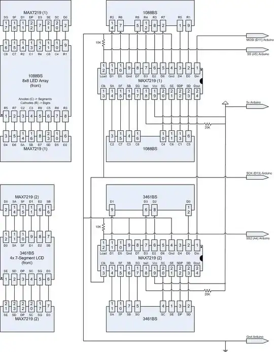
If I drew this diagram, with the ICs side by side, and the pins in the correct place, as it would be on the breadboard, it would just be an unusable mess.
What is the ‘correct’ way of drawing this kind of design? And would the ‘correct’ way be more beneficial to me as a guide to laying out breadboards? (and later on vero-boards)
The more I think of it, the more I'm thinking that it may not be possible to achieve, and I should change my approach to the problem rather than creating yet another drawing.