3

My question is this one, how the firsts ic's were produced.

The first IC was produced by jack kilby: http://en.wikipedia.org/wiki/Jack_Kilby

Now exists advanced machines, that do all the work. From cutting the wafer to make the ic.

I would like to know what type of machines they used to fabricate the IC, what techniques they used, etc.

If someone could explain me i would be very grateful

ThisGuy
  • 51
  • 2
  • For part 2 of your question: http://electronics.stackexchange.com/questions/67598/how-are-integrated-circuits-fabricated – Chris Laplante Jul 21 '13 at 22:56
  • good shared, this is very helpfull, and my discovery 2 years ago, i get the same process as your post Flip Chip Processing : https://www.youtube.com/watch?v=0ljUN0DFs8g Wire Bond Processing : https://www.youtube.com/watch?v=9hEMab3pRpU – Nilon Oct 28 '14 at 08:00

1 Answers1

5

The first thing to realize is that the first integrated circuit was not a very complicated circuit. It maybe had one or two transistors, a few resistors, and a capacitor or two.

My evidence is a photo of the first IC at Wikipedia:

enter image description here

You can see there's only 4 or so contacts to the circuit. Kilby's 1959 patent also indicates this level of complexity, although several different "realizations" are shown and its not clear which of these was actually made first.

And using the microscope slide that the chip is mounted on for scale, you can estimate that the size of the components is likely in the millimeter scale, not the submicron scale of current ICs.

The patent does give some information on how the circuit was made:

enter image description here

enter image description here

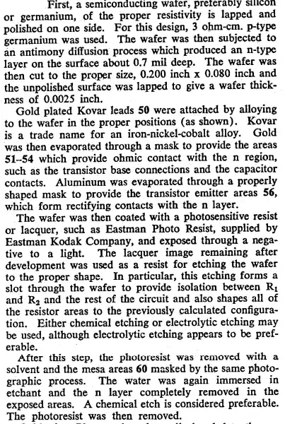
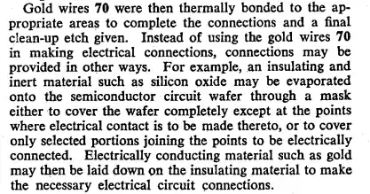
This shows that the diffusion was done uniformly over the whole wafer. The Kilby patent also refers to a Bell System Technical Journal article from 1959 that gives more details on how individual transistors were fabricated at that time. Kilby would have done his diffusion steps using a reactor designed for manufacturing individual transistors.

Different devices were isolated from each other by etching through the diffusion layer. Given the scale of the devices, the photolithography steps to define the etched shapes could probably have been done with ordinary photographic equipment.

The Photon
  • 126,425
  • 3
  • 159
  • 304
  • Do you know where i can get some images of the machines used and how can i see how they work? – ThisGuy Jul 24 '13 at 15:12
  • @ThisGuy, no idea. Go to Dallas and visit the TI museum? Look for papers published by Kilby and his coworkers at that time and see if there's photos? Look for Scientific American and Popular Science magazine articles about semiconductors from those years? – The Photon Jul 24 '13 at 15:54
  • Unfortunately for your research, most semiconductor companies keep the details of their process as trade secrets and don't share them. At the time of Kilby's work, that would have probably included the details of their shop-built equipment. – The Photon Jul 24 '13 at 15:55
  • On the other hand, nowadays vacuum chambers and things that could reproduce this kind of product are used in undergraduate instructional labs. You could probably drop by your local university (on a tour day, or during Engineer's Week or whatever) and take a tour where you'd see equipment that's more sophisticated than what Kilby used. – The Photon Jul 24 '13 at 15:57
  • Ok, thx for the reply The Photon – ThisGuy Jul 26 '13 at 11:39