8

I have heard that the clock circuit is a noise source and that the clock circuit is also sensitive to noise. I believe that keeping the clock circuit close to the MCU and keeping other routes or circuits far from clock circuit is always better.

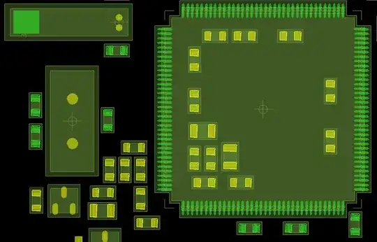
In my design, there are many wires on a four-layered PCB. The layout of the MCU(STM32)with crystals is shown below, without routing. The MCU is placed on the right of the image and the two crystals are placed on the left. Crystal 1, Y1, is 32.768 KHz, and placed on the top left corner. The Crystal 2, Y2, is 8 MHz and placed below Y1.

PCB no routing

The second image shows all routing of this part of the PCB. The thin green lines across Y1 are responsible for communication between the MCU and the CPLD. Signals up to 72 MHz will go through these lines. The thick green lines below Y2 connect the ADC module of MCU and analog signals will go through these lines. The thick yellow lines on the bottom left corner are responsible for analog power and the analog reference of ADC module of the MCU.

PCB metals 1 and 2 routing

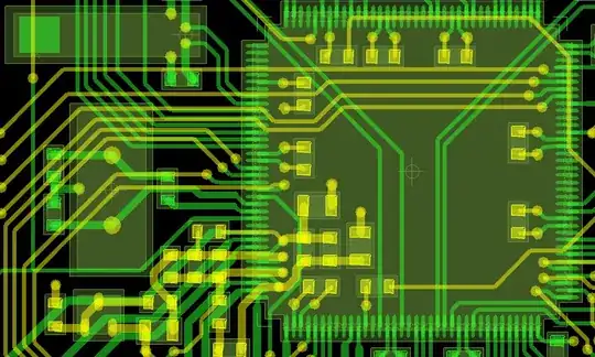
What a mess it is. I am concerned about the functionality of the PCB, especially from EMC problems. Can anybody give some suggestions on how the PCB can be improved?

travisbartley
  • 4,823
  • 3
  • 23
  • 41
oilpig
  • 843
  • 2
  • 17
  • 24
  • http://electronics.stackexchange.com/a/5608/7036 Post shows the guard ring around the xtal. Related, but probably not a duplicate. – Nick Alexeev Jul 11 '13 at 05:42
  • Which layer(s) do you have power and ground on? I would really help if you could take these images and add component idents on and indicate on the picture either with colour coding or text what your words are referring to. I can see the xtals ok but your words talk about thick tracks and I'm not sure which these are. What is the series component that swaps the xtal wires over? Two images are a minimum. 1st image not required, last image not required plus knowledge about earth/vcc planes – Andy aka Jul 11 '13 at 07:14
  • @Andyaka the structure of my PCB is SIGNAL-GND-POWER-SIGNAL.I just mentioned the location like thick tracks on the left bottom corner. next time, i will add some arrows to image – oilpig Jul 12 '13 at 04:25

2 Answers2

8

I'd like to chime in with a bit of perspective: you're not really dealing with anything high speed here. You can really do whatever you want at these frequencies and get perfectly fine signal integrity. A couple of MHz, even a couple tens of MHz, won't cause any real trouble.

Especially on the crystal side of things, you don't have to worry about a thing. I've had layouts where the crystal was placed several inches away from an MCU, and it worked just fine. I probed it, it looks just like the crystal is tightly coupled. High speed design is 300MHz and up - or high impedance from about 100MHz. That is roughly the point where routing can start causing clock skew, reflections and where your PCB traces won't behave as resistive elements anymore.

In any noise-sensitive design, you want to consider that:

  • Electric fields and especially their rate of change should be minimized. Electric fields are proportional to voltage and inversely proportional to distance, so you want to maximize spacing between lines that swing their voltage rapidly
  • Magnetic fields should be minimized. Magnetic fields are proportional to loop size and rate of change of current, so you want to decouple anything that has a high rate of current change (power conversion, IC power lines) with suitable capacitor values and you want to route power lines as closely together as possible to minimize the size of the current loops
  • High impedance means low noise immunity. Avoid high impedance lines, and if you have them, make them as unsusceptible to noise as possible. Shield them, guard them, but ideally just terminate them with a low impedance so you don't have to deal with it.
user36129
  • 8,268
  • 29
  • 37
  • Sorry. but I don't reach to understand why you say that "High impedande means low noise". Could you please explain it? – Jesus Castane Jul 11 '13 at 13:02
  • @JesúsCastañé high impedance line means a thinner line, under same conditions, it also means higher voltage level coupled from other traces. it may diturb logicl of signals. but user26129. traces of clocks should use thinner line to decrease the whole stray capacitance – oilpig Jul 12 '13 at 04:36
  • High impedance means low noise *immunity*, i.e. it's more sensitive to noise. Any magnetic or electric field coupled into such a line has an easier time disturbing the signal if it is high impedance. – user36129 Jul 12 '13 at 10:36
  • @user26129 but what it the reason of that. What is the different with a low impedance track? – Jesus Castane Jul 12 '13 at 12:04
  • 1
    You can model magnetic interference as a tiny current source (µA or nA) that gets added to the signal line. The higher the impedance of the line, the higher the voltage that is introduced by this current. Same goes for an electric field: this causes a voltage to be excited which diminishes with current. – user36129 Jul 12 '13 at 15:19
5

Prioritize your clock lines by doing these in order:

  1. Place the clock source and supporting devices
  2. Surround clock source with all the clock sinks
  3. Place any essential power structures
  4. Route the clock nets first
  5. Route other signal nets last
  6. Fill in excess area with power structure etc

One of the keys to having good routing is good component placement. You should squish the clock sinks as close as you can to the source while having enough room for shielding for noisy or sensitive components. If you finish the first couple steps and cannot move forward, you may need to rip up and reroute.

This order will place your clocks at the highest priority so your clock lines can be as short as possible. Short clock lines means less EMI between signals, so better signal integrity and reliability. Also shorter lines means a smaller capacitive load needs to be driven resulting in lower power consumption. The only way to make high-speed designs work is by prioritizing the clock because it effects timing too.

For more information, here are some guidelines.

travisbartley
  • 4,823
  • 3
  • 23
  • 41