1

So I'm a software engineer with the dream of wanting to build some cool robots and understand electronics as a result.

I'm currently hacking with a raspberry-pi and arduino, but mostly I'm trying to play and experiment a lot with a variety of things, just to know what pitfalls etc I will run into.

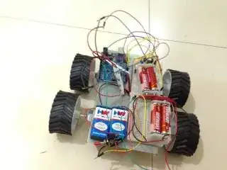
My arduino and and pi are friends over serial-usb now and I cooked a second robot with an Arduino Uno R3, it can receive commands on serial. This is what it looks like (one 9v powers the arduino, the AA holders power the motors):

Arduino Robot

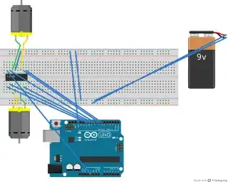
So wandering around I found out about fritzing and http://oshpark.com. I designed my board in fritzing :

Circuit Layout

I exported to the gerber files and uploaded it to http://oshpark.com, it's a pretty decent price so far!

My questions:

  • I'm a complete noob here and did this with google-fu. Is this how it is normally done? Any obvious mistakes or thing's I've missed out here?

  • I looked at the PCB layout recommendations post and there isn't a mention of fritzing, and eagle costs a $1000. Am I missing anything great without it. (For a moderately to complex robot board I plan to make)

  • I assume once this printed, it's just a flat board right? And then I will solder female headers and IC holders to connect other parts right?

  • Do I need a one-layer or two layer board? (What different would each one make?)

gideon
  • 219
  • 1
  • 3
  • 9
  • if you're just doing this for hobby work and you can live within the limitations Eagle is free. http://www.cadsoftusa.com/download-eagle/freeware/?language=en – vicatcu Jun 29 '13 at 18:00
  • aha! I see. Is there anything that eagle offers that is missing in fritzing? – gideon Jun 29 '13 at 18:05
  • [gEDA](http://www.gpleda.org/) is free as in software, without limitation. Eagle is only free as in beer, with limitations. – Phil Frost Jun 29 '13 at 18:16

1 Answers1

3

There is almost no reason to design a one-layer board these days. The entry level service for any board manufacturer will be two-sided boards with plated through holes. The only reason I can conceive of for doing a one-layer board is if you're going to etch it yourself and want to avoid connecting traces on the front to traces on the back.

I haven't used Fritzing's (what appears to be) magic for converting a wiring diagram into a PCB, but at OSHPark pricing it's worth a shot I'd say. It will either work or not depending on how sensitive your interfaces are to things like noise and trace lengths and such. But if you're wiring it up willy-nilly on a breadboard and it works, the chances of it being dumb luck are pretty low. It will probably work with whatever auto-routing Fritzing is doing behind the scenes just as well.

For the record, though, this is not the usual way PCBs are designed. Usually you'll do Schematic Entry, then you'll do Place and Route (that is placement of components on your board, and routing of traces between them). Many experienced designers will tell you that you should do the routing manually and maybe use the auto-router as an indicator of whether your component placement is OK and iterate. Once you're satisfied with your layout, you would generate Gerber files, which are vector artwork format for manufacturing. You get one file per layer, and the layers are typically:

  1. Top copper
  2. Top silkscreen
  3. Top soldermask
  4. Bottom copper
  5. Bottom silkscreen (optional)
  6. Bottom soldermask
  7. Board outline
  8. Drill file

You might also have a Milling layer, and if you're doing surface mount, you'll generate a Paste layer for the top and bottom as necessary to have a stencil created.

vicatcu
  • 22,499
  • 13
  • 79
  • 155
  • Ah thanks for your answer. So from what you said I take it that in eagle I would have to design just the PCB _manually_ ? Fritzing, does have a `design check` feature which is giving me warnings about wire's overlapping. I guess I didn't realize the logistics of the print itself. – gideon Jun 29 '13 at 18:08
  • @gideon You would create a schematic in Eagle. Then you would have a coupled board file with footprints / holes for your parts, and you'd move those to where you wanted them on the board. Then you'd draw the connections (traces) between the holes and pads on the parts (the required connections are specified in the schematic, and the CAD tool will show you in the layout what remains to be routed as an "airwire"). – vicatcu Jun 29 '13 at 18:14
  • 1
    @gideon - You expect the computer to route a board *automatically*? That's about on-par with a computer writing significant amounts of Code for you. Yes, there are things like code-generators (and autorouters), but neither will work that well without a **lot** of babysitting and instructions, and you can almost invariably get better results by doing it manually. – Connor Wolf Jun 29 '13 at 23:46
  • @ConnorWolf Yep. Now I get it. Most of the auto routing got the routes wrong, but fritzing does allow you to make manual ones. I will give eagle and gEDA a shot and see where it goes :) – gideon Jun 30 '13 at 14:32