14

I am designing a electrical device for a research project (I'm a PhD student, but unfortunately not EE!). More info on the device can be found at http://iridia.ulb.ac.be/supp/IridiaSupp2012-002/

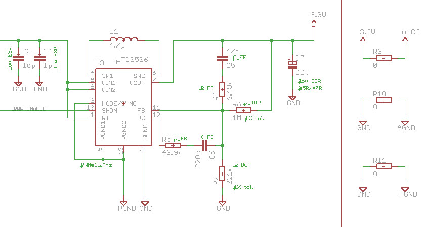
The last prototype had a problem with the power supply, and thus I tried to overcome the problems by designing a new and better one. As the device is powered by a Lithium-Ion battery, I decided to use a LTC3536 buck/boost switching regulator: http://cds.linear.com/docs/en/datasheet/3536fa.pdf

I basically used the reference implementation (page 1 of the datasheet) for a 1A/3.3V power supply as seen here: schematic
(source: ulb.ac.be)

There are three separate ground planes: PGND, coming from the battery, GND, the normal ground, and AGND for analog sensors etc.

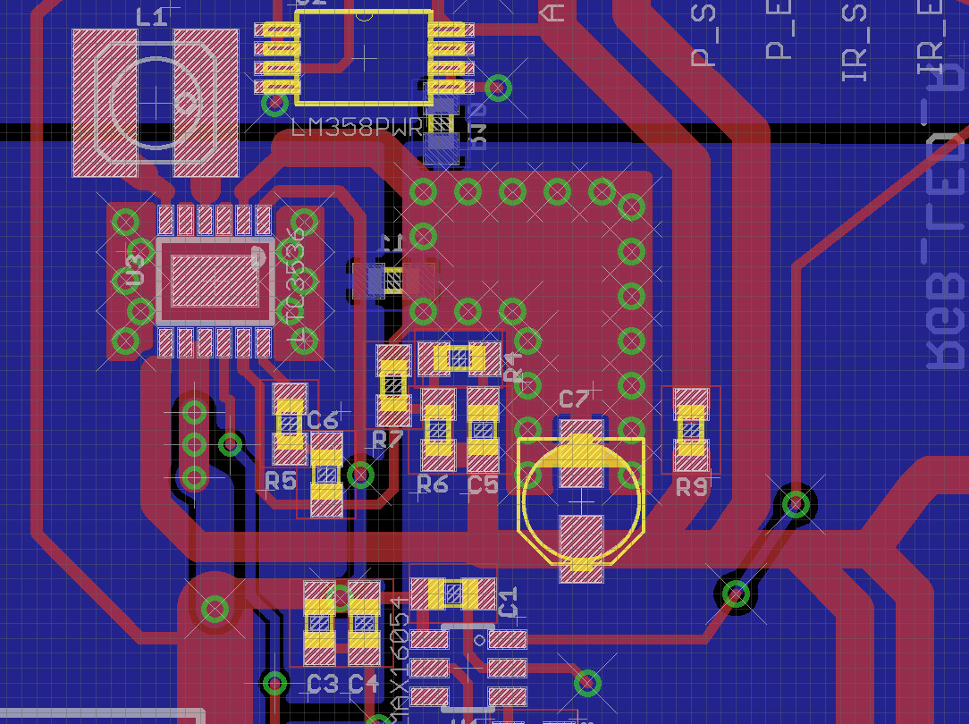
This is the board as I designed it in Eagle. I already noticed some deviations from the reference design, for example, C3 and C4 should be places a lot closer to the LTC (U3): board
(source: ulb.ac.be)

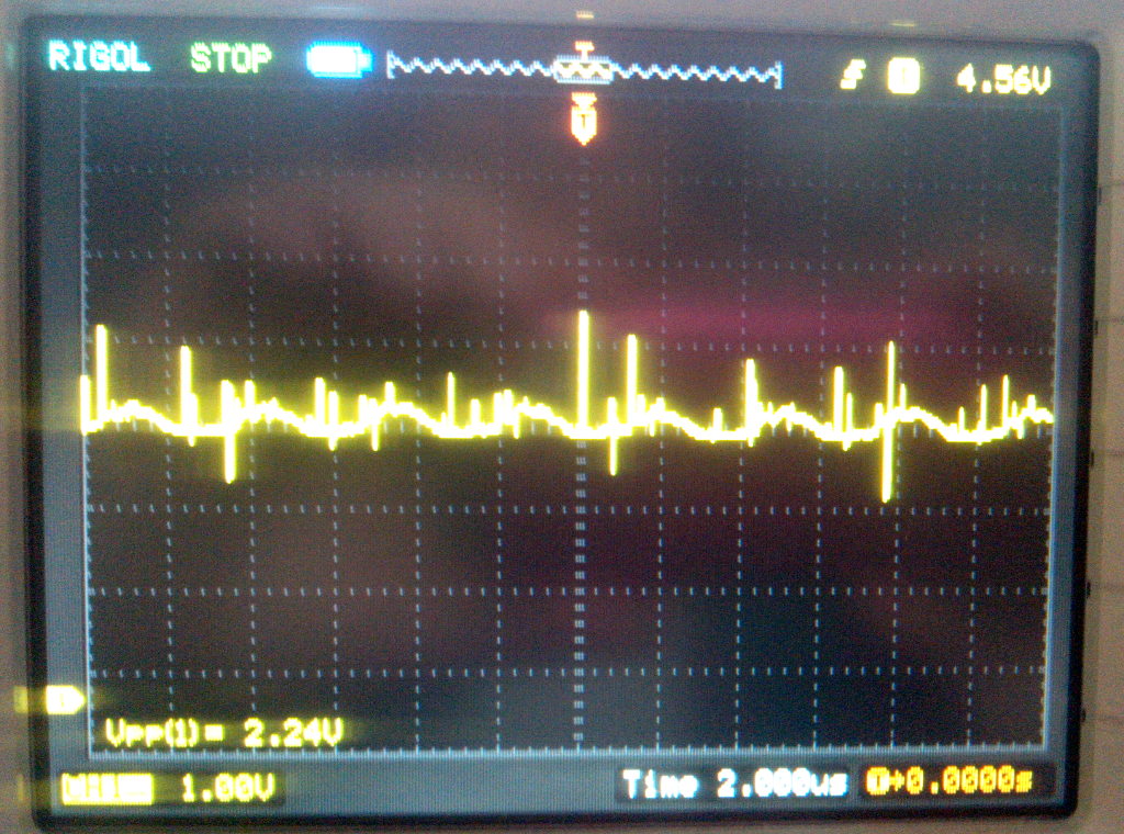
This is the output that I see on VCC (with or without load, Vin=4.7V) As you can see, Vpp is huge! It's smaller for Vin<4.3V, but still quite substantial. spikes
(source: ulb.ac.be)

I did a bit of trial-and-error by moving C3 and C2 closer to the LTC, and adding in another 1µF cap to C7. This didn't help much. I then replaced C7 with a 220µF cap instead of the 22µF mentioned in the datasheet. With this, Vpp is ~200mV. This is a lot better but still a long way from what is specified in the datasheet. Additionally, this is only the case for Vin>4.3V; below this threshold Vpp is still over 2V. I guess it's the boost vs. the buck regulation that makes the change, but I don't really see how I can correct it.

Now the questions:

  1. I was wondering if I made a mistake that is obvious to the trained eye?
  2. Why is Vpp so huge, when the noise given in the datasheet is only 40mV?
  3. Is there another way to fix this other than randomly dropping in different output capacitors?
Glorfindel
  • 1,245
  • 3
  • 15
  • 20
arnuschky
  • 435
  • 4
  • 11
  • Are you testing the power supply with a load on its output? Is that load similar to the load you'll have in normal use conditions? – The Photon Jun 24 '13 at 19:19
  • Yes, I used it with and without load. – arnuschky Jun 24 '13 at 21:07
  • "*Vpp is ~200mA*" - Presumably this is a typo, and Vpp is in milliVolts rather than milliAmperes. If not, please explain what you mean, thanks. – Anindo Ghosh Jun 25 '13 at 05:35
  • 2
    As well as FIXING the noise, how are you MEASURING it. Where is your scope ground? If you move the scope ground, does the displayed noise change. Try to place scope ground as electrically near the signal point as possible. The excessively enthused have been known t use a short wire from ground ring on probe nose to closest ground so gnd lead length is a few mm. – Russell McMahon Jun 27 '13 at 19:23
  • How is it shaping up performance wise and noise now? – Andy aka Jun 29 '13 at 17:59
  • 1
    Great information in this question. OP arnuschky, could you please fix the image links above in order to maintain this information in the communnity? – smoothVTer Jan 21 '14 at 16:56
  • Fixed. I accidentally deleted the files on the server. – arnuschky Feb 05 '14 at 09:08

1 Answers1

9

I think you'll have problems with your layout. C3/C4 MUST be closer to pin 1 (EDIT this should read pins8/9 not pin1). When I say closer I mean living on it! Ditto C7 - it needs to be camped right on pin 7. Now I've never used this part but this is standard procedure for this type of device.

Think about the current pulses flowing from pin 7 to C7 and the length of track between it and the IC - probably 20nH of track.

The ground return of C7 - where is it going? It's going right back to the wrong ground pin (signal ground). C7's ground should be as short as possible to pins 5 and 13 as possible without breaking trespass laws. And this should be your star-point for keying off signal ground. Signal ground should then go to your feedback components and not pass any load or C7 current at all.

I would decline testing this PCB if it was handed to me. Sorry for being abrupt but these are golden rules on switching circuits: -

enter image description here

Andy aka
  • 434,556
  • 28
  • 351
  • 777
  • Thank you for your fast reply. Sorry for the basic questions, but I am just a hobbyist, so please bear with me. :) What are "trespassing laws"? Do you have a source where I can read some background info? I also didn't understand the "dedicated Kelvin route" mentioned in the datasheet? Is this just a separate path with a smaller trace width? I will attempt to reroute the board tomorrow using your suggestions. – arnuschky Jun 24 '13 at 21:07
  • 3
    @arnuschky No problem. Trespass laws - just my sense of humour and trying to say get the devices ground line short = get the device right up to the pin on the chip. Kelvin route is a Linear tech jargon meaning use a seperate track to a star point and basically that star point is the junction of pin 5 and the pad underneath (13). Before re-routing there are a couple of things to try. Try a 10uF ceramic in two places - pin 7 to pin 13 (underneath, maybe drill a hole to feed a wire thru) and pin1 to pin5/13 - maybe use same technique. Try and see if it improves. – Andy aka Jun 24 '13 at 21:28
  • 1
    Two burnt fingers later... First thing was to correct the ground connection of C3,C4, and C7. I soldered electrolyte capacitors directly over the pins. Paths were long as I could only fit through-hole components, but still, the dependence of the noise on Vin vanished. Vpp was about 900mV. I then removed these caps and soldered a 10µF ceramic on the other side (drilling a hole) as proposed by Andy. Vpp is down to 350mV, and that even without input caps! Adding C2,C3 (1µF and 10µF ceramic caps) on the backside of pin8/9 results in Vpp~100mV. Adding a 10µF from pin1 to pin3 didn't change much. – arnuschky Jun 25 '13 at 08:22
  • The cap I added by drilling a hole was between pin 7 and pin 13/PGND plane. Next, I added the 22µF elca on the back, which didn't change anything. I just saw now that you asked me to add a 10µF from pin1 to pin5/13. I did that now, it didn't change much. – arnuschky Jun 25 '13 at 08:44
  • OK, to make things easier on my brain, what was the noise before and what is it now? – Andy aka Jun 25 '13 at 08:45
  • 2.2V vs. ~120mV – arnuschky Jun 25 '13 at 08:58
  • Have you tried this on-load and off-load or maybe the load is always connected? Sounds a good result so far - maybe you can fix-up the PCB without another iteration? – Andy aka Jun 25 '13 at 09:00
  • We have to produce ~50 pieces, thus I need to fix the PCB. Load is always connected but I can vary between 80mA and 400mA. – arnuschky Jun 25 '13 at 09:06
  • @Andyaka When you say in your reply. "C3/C4 MUST be closer to pin 1." I think It will be better if they are closer to PIN7/8/ These are the Vin pins. Do you agree? – Jesus Castane Jul 04 '13 at 12:19
  • 2
    @JesúsCastañé I am wrong but so are you!!! pins 8 and 9 are the Vin pins they need to be close to and these connect to pin 1 – Andy aka Jul 04 '13 at 14:15
  • @Andyaka/@JesúsCastañé: That's what I implemented in http://electronics.stackexchange.com/questions/74703/routing-a-buck-boost-dc-dc-converter – arnuschky Jul 04 '13 at 22:41