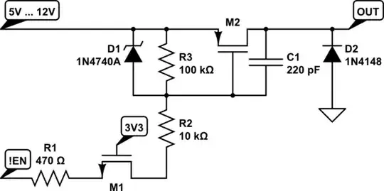
I am in the need for a high-side load switch and came up with the following schematic. High-Side voltage levels and current vary between 5-12 V / 2 A max. The high-side PMOS (SI5509DC) is rated for 20 V V_DS and 12 V V_GS and up to 4A.
A 10 V Zener diode D1 and the voltage divider formed by R2 & R3 is meant to limit the PMOS Gate-Source voltage. Diode D2 at the output shunts negative going spikes due to inductive loads towards ground.
C1 controls the fall time when opening the switch. I have not yet found a way to make the turn-on behaviour a bit smoother.
The switch will be closed most of the time and switching frequency is not an issue. However, I need to have negative logic at the input to keep the switch open during bootup when the driving pin of the CPLD is tri-stated and pulled towards 3.3V by internal pull-ups.
simulate this circuit – Schematic created using CircuitLab
My Logic interface is 3.3 V @ 20 mA CMOS (MaxV CPLD). I need to make the thing as robust and compact as possible and would like to ask for advice and comments.