8

I have a board based on an ASIC ARM Cortex-M3 that after months of work suddenly started to report spurious button presses. The ASIC is not our design, but a reputable company's.

The buttons schematic is given below. The pin is configured as input with pull-up resistor enabled. The resistor's value is about 30KOhm.

When measuring the pin-side with a DMM, I see the value floats around. Sometimes it is 3.2V (=VCC, chip range: 2.1V to 3.6V) and other times jumps around floating between 0.6V to 1.0V.

There are no issues of humidity/condensation (9% RH), no dust or other objects on traces. And this is the ONLY board that suffers this. Other manufactured clones of this board work without any issues (so far anyway).

The only thing I can think of is that something is making the internal pull-up flicker. Is it common for the internal pull-ups to give way? What else could be causing this?

Button schematic

R9,R12 are 2.2Kohm, and C10,C11 are 33nF.

MandoMando
  • 3,242
  • 3
  • 22
  • 29

4 Answers4

8

Statistics is your friend. I get it, you have a failed device, you wonder is this my fault? is it safe to ship in volume? what happens if this really is an issue and we ship 10,000 units to the field? All signs that you give a crap and that you're probably a conscientious designer/engineer.

But the fact is, you have one failure and the human foibles of confirmation bias apply to negative situations as readily as positive situations. You've had one failure, with no definite cause. Unless you know of an event that precipitated this effect then this is just anxiety.

This is ESD. Can I prove that it is ESD? - Maybe/maybe not - if you ship me the part and I spend big $$ to delid it and run it through different tests like SEM and SEM with surface contrast enhancement, maybe. I've had many cases where I deliberately zapped a device as part of ESD qualification, the device failed and yet it took a good 30 hours to find the failure point. It was important to understand the failure mechanisms and the activation energy so the hunt was necessary (if apparently wasteful) but fully half the time we couldn't see the failure point. And that was after a FMEA analysis and design guided elimination of location.

People have the false idea that ESD always means explosions and chip guts vomited all over with molten Si and acrid smoke. You do see this sometimes, but often it is just a tiny nanometer scale pinhole in the gate oxide that has ruptured. It may have happened a long time ago and over time it failed because of parametric shift.

In fact during ESD tests we use the Arrhenius equation to predict failure. We zap the devices at various levels and different models (source impedances) and then we cook the little b***rds for hours and track them over time to be able to glean the failure mode and thus predict future performance. You can easily have a 1000's of chips on boards running in environment chambers for months at a time. It's all part of "qual" - i.e. qualification.

The key effect we're always looking for for _some_failure modes is EOS (Electrical Overstress). It can be induced by ESD or other situations. I modern processes the tolerance to gate level EOS inside the chip is maybe 15% max. (That's why running the chip at it's intended MAX Vss rail is so important). EOS can manifest itself months later. The heat from operation would be like a mini accelerated lifetime test ( you're just not applying the Arrhenius equation, and it's not controlled).

If you want a better understanding look up the JEDEC ESD22 standards that describe the MM (Machine Model) and HMB (Human Body model) that describes the test probes and charging.

Here is snip of the model from JEDEC JESD22-A114C.01 (March 2005).

enter image description here

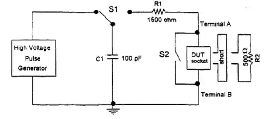
You sort of notice how it looks kinda of similar to your circuit? and the values are even kinda close, and this is used with the right voltage levels to blow the crap out of the ESD structures.

So what you need to do is:

-scrap that board
- track it's provenance, lot number and who handled it
- keep this info in a database (or spreadsheet)
- note in dB that you suspect ESD
- track all failures
- check the data over time.
- institute manufacturing controls so you can track.
- relax - you're doing fine.
placeholder
  • 29,982
  • 10
  • 63
  • 110
  • Thanks much! I have a 45V TVS across PS input (60V tolerant) and I presumed that would take care of ESD, no? reading your answer though, I believe this to be EOS or maybe ESD. This is the third board this location has roasted but the other ones were more chip-guts-vomit. The input power is a bit hot than SMPS can handle, somehow shards of ESD come through to break it. I'm very curious to know how to prevent ESD damage, I even have a [question](http://electronics.stackexchange.com/q/64588/4642) on it. If you can shed any light, I'd be happy to accept both answer along with gratitude. – MandoMando Jun 07 '13 at 20:32
  • There are probably others here that have better sense of available parts for board level ESD. I will note that while it is possible that the chip layout may differ between pads, it is notable that you got chip guts spilled, I'd suspect your board before the chip if it's localized like that. Is there something about your layout that makes those traces more sensitive? Dave TWeed's suggestions are entirely reasonable. – placeholder Jun 10 '13 at 16:51
  • well, the SMPS is rated for 40V and the input is at or just above that. I suspect the regulator lets some spikes through. The first board spilled guts, I added TVS, then it just died, I swapped the rectifier with slightly higher forward voltage to drop the input a bit and it didn't die, but this happened to it. I think EOS makes sense and the input voltage is still too high. Maybe a 3V3 TVS on the inside if the SMPS – MandoMando Jun 10 '13 at 18:24
  • (+1) I came here for something else but found this thing quite relevant to a project I am working on. My case is not this severe but I liked the logical steps required to be taken in such a scenario. I'd probably had panicked if something like this would have happened to me. – Whiskeyjack May 25 '16 at 20:45
4

It looks like you've made some effort to isolate your input pins from the switches, but still, an overwhelming ESD event may have damaged some part of the pin driver/receiver circuitry on the chip (and not necessarily the pullup device in particular).

If you want to make this more robust, you could consider adding external clamping diodes, a ferrite bead, or even a transistor buffer between the switch and the pin.

Dave Tweed
  • 168,369
  • 17
  • 228
  • 393
  • I thought about ESD, but assuming that C10 and C11 are close to the chip then it is unlikely to be ESD. The normal wisdom is that 3nF is enough to soak up most ESD events, so those 33nF caps should have provided significant protection. –  Jun 07 '13 at 16:52
  • Hmm, the ps side is depicted [here](http://electronics.stackexchange.com/q/64588/4642) could the rectifier's ground infact transient a small negative (< -0.3V) and break some clamping diode over time? Or ESD/transient coming through the pin but through the VCC. This pin is physically close to the VDD pin of the chip. – MandoMando Jun 07 '13 at 17:10
  • @MandoMando: For now, are you abole to get your board to work by kludging in external pull-ups? – Kaz Jun 07 '13 at 18:34
4

The most likely scenarios are either that the chip has suffered some damage, whose visible effects include flaky pull-up behavior, or else that code is for whatever reason causing the pullups to accidentally be sometimes enabled and sometimes disabled. The latter situation may frequently arise if main-line code does something like:

WIDGET_PIN_PORT->PULLUPS |= WIDGET_PIN_PULLUP_MASK;

and an interrupt does something like:

GADGET_PIN_PORT->PULLUPS |= GADGET_PIN_PULLUP_MASK;

where WIDGET_PIN and GADGET_PIN are different bits on the same I/O port. The main-line code will translate as something like

ldr r0,= [[address of port pullup register]]
ldr r1,[r0] ; ***1
orr r1,#WIDGET_PIN_PULLUP_MASK
str r1,[r0] ; ***2

If an interrupt happens after ***1 but before ***2, then GADGET_PIN's pullup will get turned on by the interrupt but then get erroneously turned off by the main-line code. There are two ways to avoid this problem:

  1. Make use of hardware that may allow a bit of the pull-up register to be set using a single instruction rather than a read-modify-write sequence. I believe that all Cortex-M3-based controllers provide a "bit-banging" feature that can be used for this purpose, though I've yet to find any nice way of using it from code written in C other than by manually defining bit-banded addresses. Some other processors may have I/O-port-specific means to accomplish a similar task.
  2. Disable interrupts during the port read-modify-write sequence. For example, replace the above C code with a call to a method

    void set32(uint32_t volatile *dest, uint32_t value) { uint32_t old_int = __get_PRIMASK(); __disable_irq(); *dest = *dest | value; __set_PRIMASK(old_int); }

This code will cause interrupts to be disabled very briefly (probably about 5 instructions); that's brief enough that it won't cause problems even with relatively-time-critical interrupts. Note that compiling the above method as inline may reduce the time necessary to call it, but might increase the amount of time for which interrupts are disabled [e.g. if the optimizer happens to rearrange the code so the instruction which loads the address of dest doesn't happens until after __disable_irq()].

Given that you say the pull-up behavior is intermittent, I think a code problem is probably more likely than a hardware problem. Further, damaging conditions which would harm the pull-up circuitry would be likely to cause other damage to the chip as well--some detectable and some not. If any type of demonstrable hardware damage occurs to a chip, it is almost always better to junk the chip and replace it with a new one, than to hope that the observed damage is the "only" problem.

supercat
  • 45,939
  • 2
  • 84
  • 143
0

Some of the previous answers overlook the most obvious: Check the solder joints for the button, resistors, capacitors and the uC. Under microscope you may be able to see a cracked solder joint.

If you don't have a microscope, re-solder one and one joint and see if it cures the problem.