6

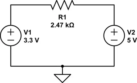
Let's assume the following scenario:

  • uC (@3.3V VDD) drives an I/O pin HIGH 3.3V (just to be clear, it's not an open-drain pin, so the p-channel mosfet of the output pin is actually driving the pin to VDD level)
  • Pin is also rated as a 5V tolerant input (so it's not clamped to VDD).
  • The line that the pin is driving is also connected to a pin of another uC(@5V VDD) which may drive the line to 5V level also
  • Between the two pins of the different uC's we assume an ~2470R resistance

The questions are:

What happens if while the 3.3V uC drives the line HIGH (3.3V), the other uC also tries to drive the line HIGH (5V)? What can then be stated about the 5V tolerance of the 3.3VDD uC OUTPUT pin?

Is then a 680uA current ( (5 - 3.3) / 2470 ) sinked to the VDD of the 1st uC? What does actually happen inside the I/O pin circuitry of the 1st uC? Is this inter-connection safe?

I post this question in case someone with a better understanding of is cares to answer, as this case is not documented in the uC datasheet and I couldn't find any definitive reference on this after doing a fair bit of research.

Nitro
  • 61
  • 3
  • Why are the two output pins being allowed to actively drive a signal in the first place? – Ignacio Vazquez-Abrams Jun 06 '13 at 14:21
  • 1
    Well, this is on an I2C bus and a bi-directional level converter is not an option (due to other constraints) – Nitro Jun 06 '13 at 14:26
  • I2C is open-drain, so you shouldn't have two outputs actively driving it. Disable one of the pull-ups. – Ignacio Vazquez-Abrams Jun 06 '13 at 14:33
  • I formulated that wrong and now I can't edit the comment due to the 5m limit. Let me try again: Well, the 3.3V output pin acts as a pull-up (through 2 resistors) for the I2C lines of a bus, and the 5V output pin on the other uC is connected to SCL or SDA of this bus. The 5V uC output pin is part of an older implementation where a different bus protocol was used. This pin may drive the whole bus directly to 5V (not open-drain through pull-up resistor). Must also mention that using a bi-directional level converter is not possible (due to other constraints). – Nitro Jun 06 '13 at 14:36
  • 2
    Irrespective of the motivation it is an interesting question that I have asked myself too. – Wouter van Ooijen Jun 06 '13 at 14:53
  • That's why I've tried to get it out of context, because I actually want to understand what happens in that case as the documentation covering this seems to be scarce. And most tell that you shouldn't do that but don't explain (or don't understand theirselves) the underlying specifics. – Nitro Jun 06 '13 at 14:58
  • @IgnacioVazquez-Abrams Because sometimes errors happen. I for one would also like to know the specifics of what happens in this case. Consider it a hypothetical. – Passerby Jun 06 '13 at 18:30
  • 1
    Can you refer to a datasheet? – jippie Jun 09 '13 at 18:52
  • Absolute maximum ratings for an arbitrary AVR state: `Voltage on any Pin except RESET with respect to Ground ... -0.5V to VCC+0.5V` and `DC Current per I/O Pin ... 40.0mA`. That would imply you mustn't pull an output higher than Vcc + 0.5V, probably limited by the internal protection diode *and* limited to max 40mA, again the current through that internal protection diode. But I'm not entirely sure if this is how it works, hence a comment and not an answer. – jippie Jun 09 '13 at 19:01
  • I don't think one can generally state that a 5V-tolerant *input* can withstand 5V when configured as an *output*. Normally, *no* device actively drives the bus lines. There are the 4k7 external pull-ups to do that. So the clean solution is to *not* output a high level at either device but to use only a low output (for 0) or tri-state the pin (for 1). Tri-stating a pin is often equivalent to re-configuring the pin as an *input* in which case it should neither 'push' nor 'pull' on the bus lines. – JimmyB Jun 10 '13 at 11:08
  • "Level-shifting" can be achieved with only two FETs, by the way: http://letsmakerobots.com/node/34444 – JimmyB Jun 10 '13 at 11:31
  • Isn't this question to broad? In the end, it totally depends on the circuit implementation inside the controllers. So without datasheet/controller type its all speculation. – Rev Jun 11 '13 at 20:13
  • I think you're right on the broadness of the question. I am referring to an STM8L151R6 uC. The reference manual includes an I/O pin schematic, however, it doesn't detail on this scenario. If you check the quoted schematic you'll see the high-side mosfet (p-channel buffer). What I suspect to be happening is that the 680uA current described above is sinked throuh the high-side mosfet (through MOSFET's intrinsec diode - pn junction) to VDD. – Nitro Jun 12 '13 at 08:58

2 Answers2

1

In the most abstract sense, what happens is this:

schematic

simulate this circuit – Schematic created using CircuitLab

You have a difference of 1.7V across 2.47 \$k\Omega\$, and so a current of about 0.69 mA flows from V2 to V1.

The line is not diven to a clearly defined state. On the left of R1, the level is whatever V1 is putting out. On the right, the voltage that of V2. Throughout the body of R1, there is a blend from V1 to V2. Obviously, this is probably not useful behavior for digital circuits where we want a defined logic level on a given signal line: the same level on both sides of any resistor.

The worst case current of about 2 mA occurs when V1 is driven low, and V2 is at 5V. From V2's perspective, it's just driving a 2.47 \$k\Omega\$ resistor to ground, but V1 has to sink the current. In the opposite case, V2 has to sink somewhat less current from V1.

Kaz
  • 19,838
  • 1
  • 39
  • 82
0

I don't think you'll find a spec on this. Some drivers can sink (and source) more current than others. Some are protected and some aren't. It depends on the types used by the die designers. To save money some versions of the same IC might have different drivers throughout its production cycles.

The 680uA current tries to sink into the VDD of the 1st uC. What happens depends on the type of output drivers on the die. Some drivers have some reverse voltage protection which feeds back to the supply of the circuity of the die some output drivers don't and can fail.

On a protected driver the current is shunted to the rest of the circuitry on the die. If it can not sink the excess current then it starts to raise the internal Vdd supply voltage. This can sometimes damage things unpredictably.

There are a few drivers that protect under both conditions where the internal circuitry is isolated and the driver is protected, however this is often not the case (follow patent trail on link to see more examples). Output drivers for pins take up a lot of die space and are often minimized.

user6972
  • 1,517
  • 9
  • 13
  • 1
    I agree with your opinion. However, I would like to know what happens on a lower-level. In this case, I am referring to an STM8L151R6 uC. The reference manual includes an I/O pin schematic, however, it doesn't detail on this scenario. If you check the quoted schematic you'll see the high-side mosfet (p-channel buffer). What I suspect to be happening is that the 680uA current described above is sinked throuh the high-side mosfet (through MOSFET's intrinsec diode - pn junction) to VDD. What's your opinion on this? – Nitro Jun 12 '13 at 09:06
  • [Section 9.3.6](http://www.st.com/st-web-ui/static/active/en/resource/technical/document/datasheet/CD00284933.pdf) shows they tested non-tolerant pins to +/- 5mA without any internal failures. However they also state "above VDD (for standard pins) should be avoided during normal product operation". I couldn't find the schematic you mention, but often they are simplified for publication. Call/email an STM application engineer. But in general if the specs say don't do it...as you noted the pn junctions are what usually get fried. If your 3V uC drives low it will sink even more current ~2mA. – user6972 Jun 12 '13 at 17:49