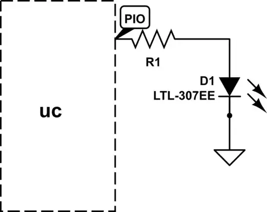
The first and third methods you show are fine, assuming the resistor is sized so that the 8 mA maximum port pin current is not exceeded. The difference between these two methods is whether the low or high side drive transistor in the processor is in series with the LED. Sometimes the low side transistors are a little more beefy, which is why you see method three more than method 1. However, either method is fine as long as you take care to not exceed the current spec for the pin. Also note that some processors have a total current spec that must not be exceeded. For example, you could have 10 pins each driving a LED at 8 mA, which would be fine individually for each pin. However, if the overall processor spec is that all I/O pins together can't source our sink more than 50 mA, for example, then you're still out of spec.
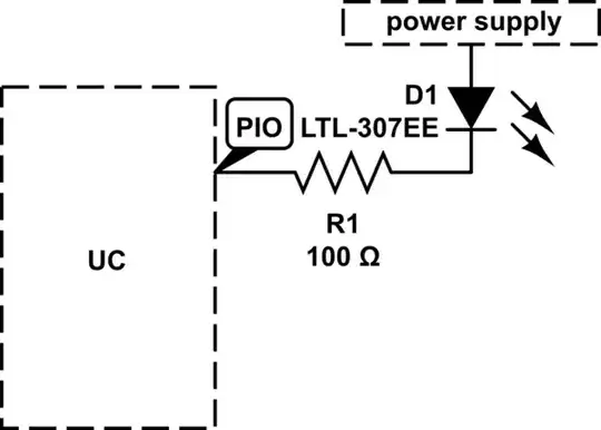
Your method two is wrong as drawn. It will likely damage the LED or transistor. To fix it, add a resistor in series with the LED so that the LED current does not exceed its maximum rated value. For example, let's say the LED is rated for 20 mA max, and it drops 2.1 V in that case. With a 9 V supply, that leaves 6.9 V accross the resistor and the transistor. The saturation voltage of the transistor is probably around 200 mV, but for worst case analisys let's just say it's 0. 6.9 V / 20 mA = 345 Ω, so the next size up common value of 360 Ω would be fine. Working backwards, and this time assuming the 200 mV drop on Q1, the LED current will be 6.7 V / 360 Ω = 18.6 mA. Even in a side by side comparison, it will be difficult for humans to distinguish that from the brightness achieved by 20 mA thru the LED.
Here is yet another method, which is useful when there is a external supply available that is a bit more than the processor voltage plus the LED drop:
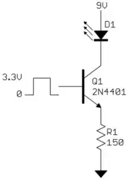
This uses the transistor as a switchable current sink, so the exact power voltage (9 V in your case) doesn't matter over a wide range. When the base is 0, the transistor is off and the LED is off. When the base is driven to 3.3 V by the digital output, the emitter will be about 700 mV less, or 2.6 V in this example. The current thru R1 will therefore be 2.6 V / 150 Ω = 17.3 mA. Since most of this current comes from the collector due to the gain of the transistor, that will be the LED current to a reasonable approximation.
Note that the 9 V supply voltage didn't enter into the calculations. As long as it is above a minimum value, the transistor will sink very nearly the same current because the transistor gain changes little with collector voltage. If we give the transistor about 700 mV C-E voltage so that it is nicely in its linear region, then the supply must be at least the digital output level plus the LED drop, which comes to 5.4 V in this case. That means the "9 V" supply can vary down to about 5.4 V without effecting the operation of this circuit.
The maximum allowable supply is limited by the power dissipation in the transistor. Let's say we want to keep it to 150 mW or less. 150 mW / 17.3 mA = 8.7 V, which is the maximum C-E voltage for the transistor when it is on. Since R1 will drop 2.6 V and the LED 2.1, that means the supply can't exceed 13.4 V. So this circuit will work nicely and run the LED at the same brightness even if the "9 V" supply ranges from about 5.4 to 13.4 volts.