9

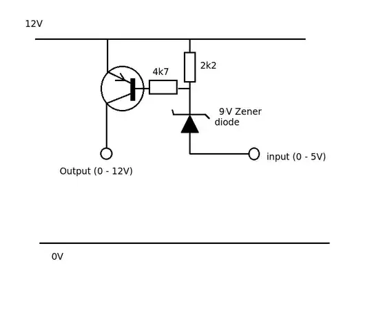
I’m trying to switch 12 V (max 30 mA) with a signal from a MCU that I’d prefer to be active low (so the output voltage is 12V when the control signal is 0 V, and 0 V when the control signal is 5 V).

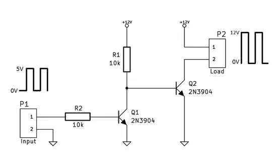
Since I have plenty of bipolar transistors at hand, I’m looking for a solution using bipolar transistors. For an active high signal, I found an answer on this site which seems to work perfectly, and it seems this can be adapted to an active low signal by adding yet another PNP transistor:

schematic

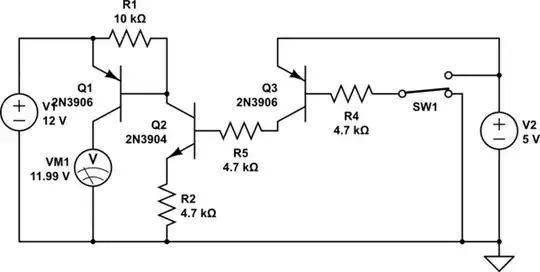
simulate this circuit – Schematic created using CircuitLab

However, 3 transistors for what seems to be a fairly simple problem seems a bit excessive. Is there a better solution?

Null
  • 7,448
  • 17
  • 36
  • 48
microtherion
  • 1,571
  • 2
  • 11
  • 18

3 Answers3

12

How about this for an idea.

With the input at 5V no current can flow through the zener (5 + 9 > 12). The output PNP transistor of held OFF by the base emitter resistors (= 4k7 + 2k2) and the output is 0. When the input is pulled down to 0V a small current will flow through the base and the 2k2 resistor. The junction of the two resistors will be a 9V (the zener voltage) and the base will be at 11.4V (assuming a 0.6V Vbe drop). The total current flowing through the base and zener (sink current) will be added (Kirchoff's current law). With values shown the base current will be 0.5mA and the resistor current 1.4mA giving a sink current of just under 2mA.

enter image description here

JIm Dearden
  • 18,926
  • 30
  • 40
  • This is a good circuit; 5+9>11.5 therefore it should work. – Andy aka May 23 '13 at 09:37
  • 1
    It is better to draw schematics so the "flow" goes from left to right (inputs on the left, outputs on the right), i.e. a mirror image of what you have now. – tcrosley May 23 '13 at 10:14
  • 5
    @ tcrosley Convention wise you are correct but I was simply trying to show the circuit in the same way that it had been asked in the question to make the comparison clearer. As was pointed out to me a long time ago - Rules are for the abeyance of fools and the guidance of wise men. – JIm Dearden May 23 '13 at 10:30
  • 3
    +1 for a different approach, rather than attempting make every problem a nail for the transistor hammer :-) – Anindo Ghosh May 23 '13 at 10:58
  • So, how would I translate this to 18v instead of 12v? 5 + 9 < 18 and do I need to adjust the resistors to keep the junction of the two resistors at 9v? – ThatAintWorking Dec 12 '14 at 22:54
8

You can achieve this with two NPN transistors as shown below. As you can see, whenever a 0V signal is given, 12V is seen in the output, and whenever a 5V is given in the input, 0V is seen on the output.

Let's see how it works. First of all, let's start with the scenario where the input is 5V, or in other words, HIGH. This will turn Q1 ON and the voltage on the collector of Q1 will be almost equal to the voltage on its emitter, which is GND. Q2's base is connected to Q1's collector, so when there is 0V on Q1's collector, or in other words when Q1 is ON, Q2 is OFF. That is because Q2's base will be shorted to ground.

When the input is 0V, or LOW, Q1 will not turn ON and can be imagined as being not connected at all. So, the current passing through R1 will turn ON Q2.

The current of Q2 is limitied with its base current and hFE, as it can bee seen in the below equation;

\$I_{CQ2}=I_{BQ2}*hFE_{Q2} = \dfrac{12-0.6}{10*10^3}*300=350 mA \$

As it can be seen, maximum current that can pass through Q2 is about 350mA. But this highly depends on hFE of the transistor, which can vary anywhere from about 50 to 300. With a hFE of 50, the current can be maximum of about 60 mA, which is enough for your specs. Lowering R1 will increase the current that Q2 will pass.

enter image description here

abdullah kahraman
  • 5,930
  • 7
  • 59
  • 104
  • Thanks for this solution! One constraint I did not mention in my question is that a high side switch would be much easier for me to deal with in the overall problem than this low side switch is. – microtherion May 23 '13 at 12:38
1

Here's an idea: -

enter image description here

Two NPNs and a PNP for the output stage. Resistor R is optional but some folk like to see one there. Make it 4k7.

With a logic 1 drive from the MCU, the middle transistor's base is shorted to ground and so collector current won't flow and therefore the output transistor will be off.

Andy aka
  • 434,556
  • 28
  • 351
  • 777
  • How could the PNP's base current ever be non-zero without R? – avakar May 23 '13 at 08:02
  • @avakar I did say it was optional but if i were being picky i'd say that with no collector current from the middle npn there will be no base current into the pnp. – Andy aka May 23 '13 at 09:34
  • @Andyaka, could you explain why this is an improvement over my original circuit? From my naive perspective, the component count of the two approaches is pretty much identical. Is the problem that my circuit would **not** work in practice? – microtherion May 23 '13 at 12:34
  • 1
    @microtherion good point - I re-read your question and now realize that you'd added the extra transistor for the inversion. OK to be a little petty is not my nature but, my circuit doesn't need a +5V connection and will work down to a MCU input of approximately 1V. Yours will still need the 5V connection and your input needs to go between 0V and this voltage (although it could be 3v3 or less). Your input does need to swing up to close the the MCU power rail to properly operate whereas mine needs to swing close to 0V to operate. Swings/roundabouts etc.. – Andy aka May 23 '13 at 13:06
  • @Andyaka, my bad, I read "no R" as "R=0" instead of "R=infinity". With the latter it makes sense :) – avakar May 23 '13 at 16:52