114

I have finally built up a lab to design electronics in. I have quite a few designs I would like to test. I have tried the printer toner/iron technique a few times but have found that I cannot create small pitch sizes as they tear off while removing the printer paper. A few people have mentioned that this is due to using a Samsung laserjet versus a HP.

I am wondering what methods you use to develop PCBs for one-offs in your lab or at home (like me). I am trying to fast track a move to SMT/SMD components and would like some tips from seasoned experts on the best PCB creation methods to test board concepts before sending them off to a PCB MFG. I would like something that balances cost, time, and beauty of the finished product geared towards a hobbyist (at this point) and geared towards SMT/SMD components.

Please include pics/documentation of your preferred method. Thank you in advance for your post.

tyblu
  • 8,167
  • 6
  • 40
  • 70
ThaKidd KG5ORD
  • 995
  • 3
  • 15
  • 22
  • 1
    As this was just flagged as a duplicate of a just closed question: I have just uploaded a 30 page group discussion on the toner transfer method to [this dropbox file](http://dl.dropbox.com/u/30808964/PCB_%20stuff.doc) Have a read through there and come back and ask relevant questions if it seems to be of use. – Russell McMahon Aug 05 '11 at 13:22
  • A [Quick Circuit](http://www.t-tech.com/) machine. It is a CNC machine that removes the copper mechanically and without nasty chemicals. – Brian Carlton Nov 23 '10 at 19:47
  • 3
    @Russell - 30 pages is a lot, and I guess it will have some noise in it too. Can't you just post the gist of it here? – stevenvh Aug 05 '11 at 14:18
  • 1
    Much noise. Conversational style. Treasure for some, dross for others. Someone using their brain can subset it in moments compared to the time it would take me for unknown benefit. I went so far as to use GMail to concatenate the thread and made a Word document from it and posted it in dropbox. In the time it took me to do that the question had been closed. I have built it. If they care they will come :-). If not then that's fine. – Russell McMahon Aug 05 '11 at 14:25

8 Answers8

76

For one-offs or prototypes I use:

  • Press-n-Peel transfer film with a laser printer (the blue one)
  • Steel wool and detergent to clean the PCB blank, then a short etch in ammonium persulphate: that gives a very clean surface, important for a good transfer from the film
  • A laminator to transfer the pattern to the PCB; I modified the laminator to raise its operating temperature a bit, and the PCB is a bit thick for the laminator but it works
  • Ammonium persulphate made with hot water in an ice-cream container, and that sits in a bath of hot water (a larger ice-cream container)

This gives good results down to 10 mil trace widths; could probably go finer but haven't needed to yet.

For double-sided boards I tape the two layers of Press-n-Peel film to two scraps of PCB at the edges so that I can get the two layers well aligned, then put the PCB blank in and feed it through the laminator. Here are some pictures to illustrate:

alt text 
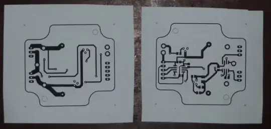
The bottom (left) and top (right) of a simple double-sided board (the top one is printed out mirrored so they overlay when its turned over). Normally I would print onto the blue Press-n-Peel film, just using paper here for illustration.

alt text 
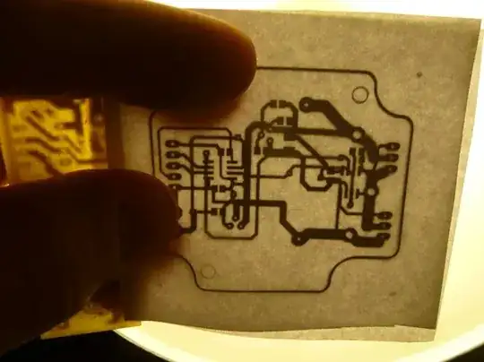
With one side taped to the scrap PCB (left side) and the printed sides facing each other, hold them up to the light and align the other one so that all the holes and the board outline line up.

alt text 
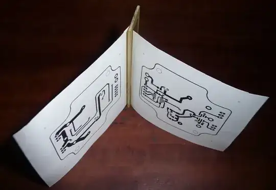
Here they are both stuck to the PCB scrap. You can now put the clean blank PCB between the two (probably best to tape it to both sides to avoid any movement) and run it through the laminator (or iron it) to transfer the toner onto the PCB.

You can tape the two pieces of film or paper together without using the scrap of PCB, but when you put the blank PCB between them you can get some relative movement as they flex around the thick PCB. With the scrap piece the same thickness as the blank PCB they stay in the right place.

A bench drill is good for any drilling. I use drills down to 0.5 mm diameter but with 3 mm shanks so they are easily held in the drill chuck.

For through holes I solder thin copper wire to the pads on either side. The wire comes from a multi-core flexible cable; individual strands are or about 0.2 mm or 8 mil diameter. This takes some time!

And to solder I place solder paste with a fine-tipped syringe, place parts with fine tweezers then reflow in an electric frying pan. A few more pictures:

alt text

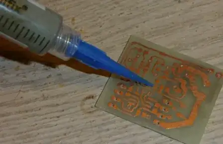
Syringing solder paste onto SMD pads.

alt text

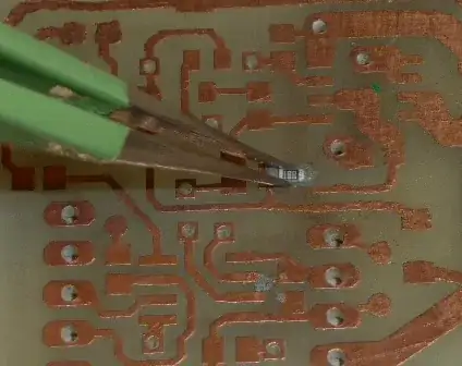
Placing component with tweezers

alt text

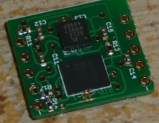
A finshed board - the PCB was professionally made but I assembled components and soldered as described here. These are 0402-size resistors and capacitors (quite small, amazingly easy to lose), an accelerometer in a QFN-16 package (4x4 mm) and a memory chip in an 8 pin leadless package, similar size to a SOIC-8. (This is part of a small accelerometer data logger, see vastmotion.com.au).

Good luck!

John Gallant
  • 681
  • 5
  • 9
  • 1
    Could you describe in a bit more detail the method you use for double sided boards? Do you have pictures of your process or a link(s) you perfected your process from? Also I would be very interested in more details concerning the use of solder paste. Thx! – ThaKidd KG5ORD Nov 22 '10 at 09:29
  • 2
    Yes, that was a bit sketchy! I've added some pictures to illustrate the process. – John Gallant Nov 22 '10 at 11:15
  • 3
    Excellent answer John. Hope this takes top spot. – Mr. Hedgehog Nov 23 '10 at 22:32
  • 3
    syringing solder paste is kind of slow. Your local hardware store probably has some sheets of 0.003" or 0.005" brass shim stock. If you etch it like a PCB you can make a stencil with it. Here's a picture of a stencil I made: http://imgur.com/UulSo (This one has been used on about a hundred boards.) more here: http://www.delorie.com/pcb/brass/ – markrages Nov 24 '10 at 03:24
  • 2
    What is "press-n-peel transfer film" called in stores? Googling finds lots of things called that, but none market themselves for PCB fabrication. – Cerin Oct 30 '15 at 22:13
  • 1
    Where did you find a laminator that could handle something as thick as a PCB? All the ones I see support a max thickness of 5 mils, whereas most PCBs are 300-600 mils. – Cerin Oct 30 '15 at 22:35
  • @Cerin [This is the one I use](https://www.amazon.com/dp/B00LV3KESI) (no affiliation). I've used it with 0.8 mm boards; others have reported using that specific model with 1.6 mm boards. – Alex Hajnal Dec 16 '21 at 06:50
59

Unless you're on the tiniest of tiny budgets, just have the boards professionally fabbed.

Really, you can get such a good deal on PCBs, with suppliers like:

  • 33Each.com — 60 Square inches, double sided, 6/6 spacing. $33 ea, minimum order: 4 (1 if you have a university address)
  • GoldPhoenix — Good for bigger runs, cost varies depending on requirements.
  • ExpressPCB — 3 boards for $51 total, double sided, no soldermask or silk, rigid size requirement of 3.8 × 2.5
  • AP Circuits — No personal experience, see comments below.
  • Sunstone Circuits — As cheap as $28 for a prototype. Fast and good quality, I've never had a problem (From Garrett Fogerlie).
  • OSH Park — $5 Sq. In double-sided, $10 Sq. In, 4 layer. Boards come with purple(!) soldermask.

On the whole, I've found that (for me, at least), it's just completely not worth it to try and make my own boards, when I can buy a much nicer board or ~$50.

Also, with most professionally fabbed boards, you get all the niceties, like soldermask and silkscreen. Having a soldermask makes soldering small pitch components far easier, and the silk makes populating components much easier, particularly when boards get large.

How much is your time worth to you?


Edit: Removed BatchPCB from the list since they no longer exist (sold to OSH Park in 2013).

hlovdal
  • 999
  • 1
  • 13
  • 21
Connor Wolf
  • 31,938
  • 6
  • 77
  • 137
  • 22
    I can have a board ready for assembly in under an hour. At £30 an hour for my time, it's very cost-effective for me. I could get a nicer board made for that, but I'd have to wait a couple of weeks for it. – Leon Heller Nov 20 '10 at 13:02
  • 8
    Fake Name: I agree that you can get great results from a pcb mfg...however, I have to go with Leon on this one. If I get a wild hair up my ***, I want to be able to build it out in a few hours versus waiting 2+ days. If I am going to make a few of them, however, I am definitely sending the PCB to the MFG. – ThaKidd KG5ORD Nov 20 '10 at 17:28
  • 4
    @Leon Heller - Under an hour? Really? Including drilling? I guess your boards have fewer holes than almost all my projects. – Connor Wolf Nov 21 '10 at 04:08
  • 5
    @Fake Name: SMT is the future. – Mr. Hedgehog Nov 22 '10 at 16:44
  • 2
    I still need at least 20 vias on my most basic boards. – Kortuk Nov 23 '10 at 17:23
  • 4
    If you can spend 'n' days prototyping, drawing a schematic and laying out the components - I don't see why you can't spend an hour or two making a board. You guys must have the patience of a rock because when I have finished my design I want nothing more than to hold the finished board in my hands and try it out. – Mr. Hedgehog Nov 23 '10 at 22:28
  • Hurrying can ruin *anything*. – Connor Wolf Nov 24 '10 at 09:31
  • @Mr. Hedgehog - The boards I am talking about are *entirely* SMT. I guess I just do complex stuff. – Connor Wolf Nov 24 '10 at 09:32
  • 5
    Anything that I could make that needs a single layer of copper I can do with veroboard and point-to-point wiring. Anything else I have sent out to either apcircuits.com (single/double layer, extremely fast turnaround) or sunstone.com (multilayer, larger boards, higher volume). It's not worth my time to try and etch my own boards, *especially* double-sided. – akohlsmith Nov 24 '10 at 14:12
  • @AndrewKohlsmith, I had not seen apcircuits before, they are perfect if you just want 2 simple ones. Sunstone is pretty affordable for lightly larger number.@FakeName, will you add them to your list of good suppliers? @FakeName, on the note of board complexity, I use SMD almost exclusively and have many vias just to number of components. – Kortuk Nov 25 '10 at 17:30
  • 2
    I've had a few boards made from the DorkbotPDX PCB Order (http://dorkbotpdx.org/wiki/pcb_order) they batch up orders similar to BatchPCB and send full panels to fab. Costs $5/sq inch (for 2-sided) and you get 3 copies of your board. – Craig Jan 19 '11 at 12:29
  • 2
    I must also mention that I have ordered boards from DorkbotPDX. They turned out quite nice. Laen even spotted a problem with a board and spent the time to explain what I had done wrong in Eagle. Great service and great pricing. Would recommend DorkbotPDX to anyone. – ThaKidd KG5ORD Mar 31 '11 at 07:16
  • @AndrewKohlsmith - untrue. The specific thing you can do with a custom prototype PCB is put footprints for fine pitch parts exactly where you want them. You can get premade boards with most footprints, but you'll either be sawing up board stock and gluing it where you need it, or have a prototype that is much larger mechanically than the end result. Being able to put the prototype in it's housing can be key sometimes. Even testing the assembly challenges of a board you are also ordering at the same time can sometimes be worthwhile. – Chris Stratton Jan 09 '13 at 20:32
  • @ChrisStratton it's very rare that I need a *prototype* to be both mechanically and electrically close to final. I usually want my mechanical prototypes to test fit/form and electrical ones to have lots of breakouts and be able to get at everything. – akohlsmith Jan 10 '13 at 03:54
  • 1
    @AndrewKohlsmith - I often need my prototypes to be both electrical and mechanical matches, so that I can demonstrate the end result exactly as it would be used, and verify that there are no interrelated electrical/mechanical issues. Prototypes made of larger proto boards tend to be quite unwieldy - I'm efficient enough at making custom ones that I tend to avoid that, though I've been known to make breadboarding adapters for footprints I didn't have on hand in order to *experiment* with circuitry around a new component. Sometimes, I'll send a PCB order and also make one the same day. – Chris Stratton Jan 10 '13 at 15:03
17

I get excellent results (down to 8/8 mil) using the photo-etch technique. I use a cheap HP 5940 inkjet printer with Mega Electronics JetStar Premium film for the transparencies with pre-coated positive resist boards, exposed in a home-made UV exposure unit. Boards are developed in sodium hydroxide solution and etched in ferric chloride in a small plastic container in an old washing-up bowl with about 1" of very hot water in it. The small container is agitated manually, and etching takes about 5 minutes. I can make a board in about 20 minutes, not including drilling.

Here is one of my boards.

This group is a very good resource for making PCBs at home.

Leon Heller
  • 38,774
  • 2
  • 60
  • 96
  • 1
    So far I have used the Muriatic Acid + Hydrogen Peroxide method. How messy is the process you use? What kind of disposal is require? Thx for the link, I am going to take a look at that right now. – ThaKidd KG5ORD Nov 20 '10 at 17:31
  • 2
    Ferric chloride stains things badly. It lasts a very long time, and the life can be prolonged by adding hydrochloric acid. Small amounts used at home can be flushed down the lavatory, the copper content is minimal and ferric chloride is used by water companies. – Leon Heller Nov 20 '10 at 17:37
  • Good to know...Here in the states, I would hate to have the EPA knocking on my door. – ThaKidd KG5ORD Nov 20 '10 at 19:21
8

I'm no seasoned expert but... I have learned from them.

I have the second cheapest Samsung mono printer available and I have no problems with fine traces; I doubt it is your printer.

I have had good success with laminators but someone recently told me this could be dangerous on cheaper models with improper shielding (as the board is highly conductive).

I have returned to ironing for double sided boards as it seems to be a tad more accurate. If you're not getting good transfers try using an electric sander with a very high grit rate to get it much cleaner than any abrasive brush can. Then, the most important thing to do when using an iron is to push hard, like really hard and hold it in place for at least 30s at a time. If you have normal glossy paper and can't see the traces, you're probably not ready to soak.

Another thing I have found to help is to have a 2mm or so border around the whole circuit. This then tends to stick first and helps prevent the paper from moving while you are ironing.

Currently my kit features the following items:

My new camera arrives today and I intend to launch a "website of journey" as I both learn and experiment with electronics. One of the first videos I will put out will be my PCB production process.

Mr. Hedgehog
  • 2,117
  • 4
  • 24
  • 30
  • 1
    Interesting..I am running with the Samsung ML-2250. I have not replaced the toner in a few years. I'll try your suggestion plus replace that toner. I would be very interested in seeing your site/videos. Please leave a link in the comments when its up. Look forward to checking it out. – ThaKidd KG5ORD Nov 20 '10 at 17:23
  • 5
    I think the #1 problem anyone making their own boards has is that they don't actually start with *CLEAN* copper. Clean copper is pinkish, not copper-ish. Wash it down thoroughly and give it 15 seconds in an etchant bath, then wash it off immediately with distilled water. You'll notice the board is hot pink. This is clean copper. – akohlsmith Nov 24 '10 at 14:12
  • @ThaKidd: I added a new answer as it's related to this topic (too long for a comment). I haven't done the walkthrough yet - that'll be next hopefully. – Mr. Hedgehog Nov 28 '10 at 21:42
  • Weird, back when I was still making my own boards, pressing the iron really hard was the key to screwing it up: the toner would melt and flow sideways! Perhaps my printer deposited the toner too generously or something :) – Roman Starkov Apr 13 '11 at 10:49
  • 1
    While there are many variables, I've had great results with cheap HP printers but terribly unusable outcomes with a comparable Brother and a large whole-office Canon, using the same procedures. So I think the printer/toner definitely is a factor. – Chris Stratton Jan 09 '13 at 20:26
  • 2
    Stackoverflow seems to be breaking most of your links with some sort of sleazy tracking system. They're showing up as `http://rads.stackoverflow.com/amzn/click/` and redirect to a 404 page even though your original links still work. – Cerin Oct 30 '15 at 22:43
5

I have just finished creating a tutorial on how to build a Bubble Etch Tank (unheated), at home, with minimal cost and effort. Hopefully this will be helpful to someone:

  1. What You’ll Need
  2. Plumbing the Air System
  3. Making Bubbles
  4. The PCB Basket

I'd recommend increasing the resolution to 720p but of course, this is optional.

I'll be adding further updates (such as seeing the tank in action) at 13 Volts fairly soon.

Mr. Hedgehog
  • 2,117
  • 4
  • 24
  • 30
4

I would vote for cheap Chinese off-shore, too. iteadstudio.com can make 10 boards 50x50mm for $10, and 3-day air shipping for the order is < $30. Total turn-around time is a tad over a week. I hear that seeedstudio.com is very similar (and may actually be using the same PCB fab.) You get solder mask, silk screen, vias, plating, the shole shebang. The only draw-back is they can only do 1 oz copper thickness, and they aren't very precise at tiny pitches (8 mil is their minimum.)

For doing my own, I would recommend against the CNC mill route. Yes, it's nice that you can drill the same board you mill, but the milling generates glass dust that's really bad for your lungs, and it easily breaks the tiny bits you need, and the edge finish is kind-of ragged and not trustworthy for small pitches. Instead, I would go with UV-based photosensitive coated boards. Laser print the mask (inverse) on transparencies. Expose on a UV bed (can be built yourself if you really want to.) Develop. Etch.

Then, that CNC mill may still come in handy, for drilling the board :-) You're still not going to get through-hole plating, vias, etc, this way.

Jon Watte
  • 5,650
  • 26
  • 36
  • 2
    The only real justification for making your own is in the cases where the fact that you can design, fabricate, and test the circuit inside of a few hours of a single day is important to the progress of your overall project. Well, that and RF people and others who need exotics. – Chris Stratton Jan 09 '13 at 20:29
  • 1
    http://pcbshopper.com/ is a great place to search and compare PCB manufacturers. (I am just a user, no other connection whatsoever). – user1139880 Jan 01 '17 at 17:33
3

Thanks to everyone so far for your answers. I believe I have made a decision concerning future circuit board design. I have been doing some crazy research and ran into a piece of equipment that I believe might be the best route. It is not only eco friendly but useful in many other ways. Props have to go to Brian for triggering the research that led to the epiphany.

Instead a dealing with chemicals which requires disposal, time, and is not ideal since I live in a condo, I have decided to build a CNC Mill. There are numerous tutorials out there and it appears one can be built for ~$500 (or less if salvaged parts are used). Here are a few links I have found so far.

Instructables

Engaget (1of3), (2of3), and (3of3)

The mill would not only serve the purpose of removing the copper but can also be used to build a solder mask. This would enable easier SMD/SMT manufacturing using the skillet reflow method.

I plan on doing further research to see if a 'combo' cnc machine can be put together which also takes advantage of the RepRap 3D plastic printer. Imagine the possibilities of this killer combo. You could fabricate almost anything and it should cost under $1000.

ThaKidd KG5ORD
  • 995
  • 3
  • 15
  • 22
  • 1
    How do you plan on adding solder mask to the boards using the CNC? Are you buying pre-masked copper boards and effectively "sanding off" the soldermask for pads, then going a little deeper to remove soldermask and copper for traces? – akohlsmith Nov 24 '10 at 14:25
  • 3
    Unless you spend a lot of money, milling PCBs is very slow. – Leon Heller Nov 24 '10 at 15:33
  • @LeanHeller, @ThaKidd, We use cnc mills at my school as the simple process(also chemical etching). They are slow and the bits are expensive to replace. – Kortuk Nov 25 '10 at 17:24
  • In particular, http://reprap.org/wiki/Automated_Circuitry_Making shows a PCB that was milled by a RepRap. – davidcary Mar 04 '11 at 19:52
  • @ThaKidd please post a follow up about your experience with the CNC mill. I have a CNC mill, but have yet to mill a PCB as it seems pretty time consuming. Ad that to the fact that you can get a good proto for $100 in a few days or $20-30 in a week if you want to wait. – BrianV May 05 '12 at 16:50
  • @ThaKidd did you end up going with the CNC? What were your experiences? – Garrett Fogerlie Oct 25 '12 at 15:06
2

I wasn't getting reliable results ironing on toner transfer. I modded an old waffle iron - named the PCB Press. I like the ability to produce a prototype board at home in under an hour. If I need something of professional quality I send the tested proto out to fab house.

MarkSchoonover
  • 1,113
  • 10
  • 17