Changes in my design are forcing me to replace my 44-pin dsPIC33FFJ16MC304 with a 64-pin (same package size, finer pin pitch) dsPIC33FJ64MC506. In the datasheets for both chips, Microchip recommends a guard ring connected to ground around the oscillator circuit and a trace length of no more than 500 mils on the OSC lines.
The board is a 4-layer stackup (signal, ground, power, signal). I'm concerned about EMI because the board will be located near a compressor and two fans.
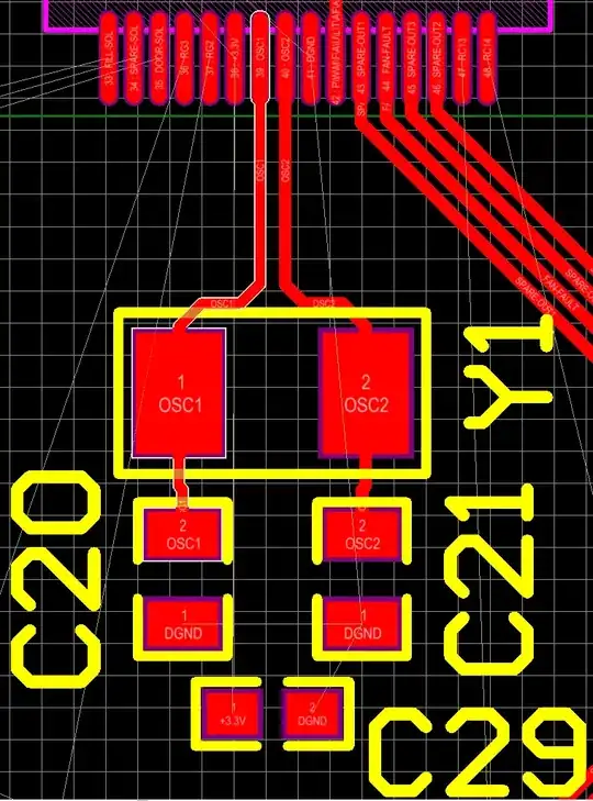
Pins 28-31 of the 44-pin package are +3.3V, DGND, OSC1, and OSC2. I currently have the oscillator circuit laid out like so:

C10 is a 0.1 uF decoupling cap, C20 and C21 are the 18pF load caps for the 8MHz crystal Y1. I put the via to the ground plane at the end of the guard trace because Altium was treating it as an incomplete trace.
The decoupling capacitor placement is not optimal per Decoupling caps, PCB layout, but ignore that for a moment. On the new 64-pin chip, the pin arrangement changes to +3.3V, OSC1, OSC2, DGND.
It seems to me that the obvious location for the decoupling cap in this case is underneath the chip, but I'm restricted to placing components on the top layer only. That being said, I'm guessing I have to have C10 straddling C20 and C21 so that the power/ground lines go around the oscillator circuit. I don't like how long that will make the traces to the decoupling cap. For optimal EMC,
- I intend to redraw the guard ring as a polygon pour to eliminate the extra terminating via. Where should I connect the guard ring to the ground plane, the single via in Olin's answer to Decoupling caps, PCB layout?
- The guard ring connects to the ground pin on the PIC that the decoupling capacitor would normally be connected to. Do I connect the ground pin of the decoupling cap to the guard ring?
- What if I avoid the longer decoupling cap trace length issue by using two caps (one for the power pin, one for the ground pin) like in How to connect decoupling capacitor when VCC/GND pins aren't close? Would this work better? My concern with this approach is how to connect the extra capacitor pins to the reference planes.
- Do I increase the length of the OSC lines to better fan out the surrounding traces? It's currently about 320 mils from the MCU pins to the load capacitors, so I do have a little headroom there if needed.
EDIT: Here's the new chip pinout, no guard ring yet. Current OSC trace length is 416 mils. C29 in the picture is supposed to be decoupling the 3.3V and DGND pins on either side of the OSC pins. The decoupling cap is now a 0603 instead of a 0805 as well.