12

For a few small 2 layers boards I'm doing, I'm using the top layer for parts and signals and a ground pour on the bottom layer with no or very short traces, based on comments and answers to my previous question

Since the top layer becomes too chopped-up with a lot of islands, which makes it practically useless and I'm also trying to minimize the current loop between the ICs and decoupling caps (if I leave the top layer it will connect to the caps and the ground pins separately and not in a single point), so I decided not to use a copper pour on the top layer at all for the mentioned reasons.

The problem with this approach is the manufacturing side of things, if I understand correctly FR4 material could wrap if the copper on both sides of the PCB is unequal (although I don't understand why that doesn't happen with a 4 layer board typical stack-up sig-gnd-vcc-sig), so I'm back where I started

I've been going back to this a lot doing a lot of research but still can't find a conclusive answer and I can't decide what to do.

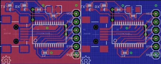
This is an example board, the one on the right without top copper pour. enter image description here 
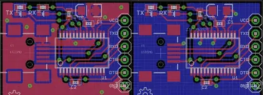
Update: based on your comments, I revised the board to avoid breaking the ground as much as possible, but still can't decide on the top layer though.

enter image description here

mux
  • 1,866
  • 5
  • 23
  • 27
  • 1
    Are you concerned about warping of the board? That shouldn't be a consideration, I've made boards that are 18" long 2 sided , soldi on one side that didn't warp. It's best to talk to your vendor about that. Seems rather a silly statement for someone to have made. – placeholder May 16 '13 at 16:04
  • @rawbrawb personally I was not that concerned, but some answers and comments here made me worry.. I'm more worried about current loops. – mux May 16 '13 at 16:17
  • Please don't read my comments as being anti-pour. I agree with @dave-tweed keep the pour! there are good reasons to keep it. – placeholder May 16 '13 at 16:23
  • @rawbrawb I'm more inclined to keep it, but I'm not sure if those reasons still hold, after placing all the components and doing the routing there's not much left of it anyway, maybe that's a bad example but other boards have small islands of copper not a pour anymore. – mux May 16 '13 at 16:28
  • I'd suggest leaving the top copper - it does not harm to have it there. Note, that in fact you have a bigger loop in the case without the top pour. Also try to route tracks so they split the bottom plane less - your VCC connection from header could be routed under the tracks from header and around the chip - this way you'd loose one jump in TXD connection making the bottom plane more solid. – miceuz May 16 '13 at 17:29
  • 2
    Is this USB pinout correct? Maybe I am looking at it wrong, but something seems off. – dext0rb May 16 '13 at 19:07
  • 1
    @dext0rb yes, I switched VBUS and GND, good catch you saved me a new PC :] – mux May 16 '13 at 19:37
  • Awesome! Wish I could get some rep for that one. haha jk – dext0rb May 16 '13 at 19:49
  • Your revised board is not the same netlist without the pour. – markrages May 16 '13 at 21:59
  • Would the chip route better if it is rotated 180 degrees? The USB connections would be shorter. – markrages May 16 '13 at 22:00
  • Actually, rotating it 90 deg CCW would make most of the connections much shorter. Also, the new version without the pour is missing a lot of ground connections. – Dave Tweed May 16 '13 at 22:18
  • @DaveTweed I thought about rotating it, but didn't want to place the parts at the bottom, will give it a try anyway, and the new version left and right are the same, the top layer is just hidden. – mux May 16 '13 at 22:30

3 Answers3

10

In general, I would say keep the top-side pour; it certainly does no harm, and it has some secondary benefits, such as less etching required and less thermal stress on the board during reflow.

You do still need to pay attention to current loops and place the vias appropriately, not just scattering them about randomly. Since the FT232R is the only active chip on the board, focus on its outputs. There are two LEDs that are powered by VUSB, and a few outputs associated with the serial port that are powered by VCC. Where do the currents flow when any of these outputs change state? Try to keep the paths as short and direct as possible.

Note in particular, the ground path for the USB connector in your non-pour example. It has to go down, cross below the chip, then come up on the right before it gets to the ground pins on the top of the chip. The top-side pour shortens this considerably. In either case, it would help if you adjusted the vias near pin 1 of the chip so that the bottom pour is continuous there.

One side point about your design: Try to avoid having three etches come together at an acute angle, like you have on your Vcc trace. Make that a right-angle tee connection.

Dave Tweed
  • 168,369
  • 17
  • 228
  • 393
  • yes I also considered the etching costs, but currently I don't pay for that, so that's not a problem, I'm more concerned about the current loops, in your opinion, which design is better ? and how can I reduce the loops with the upper ground pour ? – mux May 16 '13 at 16:20
6

In this case no copper seems better than a poor copper pour. With I2C you're not really at high frequency but the gates might be switching in about ~350ps which could still cause emf, ringing, etc.

As Andy Aka suggests, (and this answer is only meant as supplement to his), maintaining a better ground plane in the bottom is more important here and you're better off trying keep that from being broken. Notice that TXD is causing a divide in the bottom copper and makes a "bay" and disconnect around the bottom left. If you via to the gnd plane, run as short of a trace as possible.

If you do pour copper, make sure you remove anything that looks like a peninsula/bay, long dangling strip, etc; or place a via to the gnd at the tip and stitch them.

That whole L shaped copper pour around top pins of the IC looks like an antenna to me (disc: I'm NOT an RF expert) and keep in mind the emf radiation is affected by the area of the rectangle that L shape copper makes. At some frequencies (or harmonics) that thing might light up nicely.

As far as power plane decoupling properties of the copper, you'll need at least 1 sq inch of copper at less than 10 mil prepeg (gnd-vcc layer gap) to get anything going. So don't worry about it here.

Quote: They say there are two types of engineers:

"Those who make antennae intentionally, and those who make them unintentionally."

MandoMando
  • 3,242
  • 3
  • 22
  • 29
5

Firstly, there are at least three tracks I see that don't need to route to a different layer - it's fairly vital you minimize breakages in the bottom pour even if it means adding two inches (300 pico seconds) to a track on the top layer. You develop an eye for these things: -

  • TXD to pin1 can all be on top
  • X1 pin1(?) to U2(?) can all be on top
  • U1 pin 16 to X1 can all be on top
  • Pins 22 and 23 needs the vias shifting so that the bottom flood connects thru - yes I know it's fiddly but it needs to be done.
  • R2 has a blue track wandering off somewhere that seems superfluous.
  • DTR to pin 2 can be on top

OK I've said these things and one track being routed exclusively on the top may make another suggestion hard to do but you will find a better way that minimizes tracks on the bottom. GET that 0V better!!

Personally I don't care about a top pour and I'll tend to treat supply voltages to chips (for the analogue/digital stuff I do) as tracks on the top layer. However, if I see a chance when the bulk of the routing is done I may make little extra compromises to the bottom layer if it can give me decent flooding with Vcc (or another ground) on the top layer.

I'll get my routing done then get Vcc routing done and see what I can do with a top pour (if any).

sig-gnd-vcc-sig is "balanced" because the sandwich is symmetrical about the centreline of the board - this assumes that the amount of copper on the inner layers is about the same and that there isn't much in the way of big Cu stuff on one area of the outer layers BUT this is "old school production values" and shouldn't be a big concern. Obviously gnd-sig represents a lot of Cu on one side compared to the other but again it's old-school care that is superceded by better modern production standards.

Andy aka
  • 434,556
  • 28
  • 351
  • 777