6

I bought this micro usb part:

enter image description here

I need to solder it to a PCB that I designed, but I'm having a ton of trouble figuring out how to do so because the tabs are very close together and hard to reach. Is there a technique to do this / are there extraneous parts on the connector that I can remove to make it easier to solder?

Johan.A
  • 1,806
  • 1
  • 15
  • 27
user592419
  • 163
  • 1
  • 1
  • 4

5 Answers5

6

Provided your PCB already has the correct footprint, the best way to solder this is hot-air/paste or an oven.

Here's a picture of what the footprint for a similar connector (or the same, I'm not exactly sure) looks like on a board I designed recently.
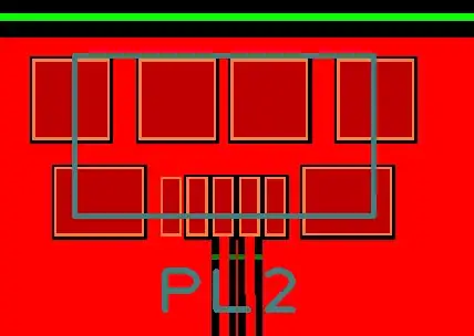
usb footprint

I soldered these connectors onto the PCBs by paste and hot-air (you can check out a quick video on what hot-air looks like here). The important thing is getting all of the contact points molten at once, otherwise you'll be stuck with mechanical stresses on the joints (which is, obviously, undesirable) or bad connections.

An oven and solder-paste could also work quite similarly. A general method for that would be to apply paste, mount the connector, put the board in the oven and heat it until the joint forms.

Shamtam
  • 3,546
  • 19
  • 27
  • Thanks for the video. I don't have the hot-air but this seems like the most suitable option. @EJP solution below also seems good, but I couldn't get it to work. – user592419 May 13 '13 at 19:48
  • EJPs solution works great for ICs (LQFPs and SOICs and such), but for this connector you will have trouble with that method, due to the mechanical connection pads (the 6 square pads in my footprint picture). – Shamtam May 13 '13 at 22:01
  • 1
    I hand solder these a lot, you can just line up the pads then tack it down with one of the mechanical pads. If you push it toward the edge of the board a little it is easier. Next time edit the footprint to make the pads longer and it is no problem at all. – Matt Aug 14 '13 at 14:13
4

I tried numerous methods and found the following to work best:

  1. Use a fine tip
  2. Flux on the connector pins and on all the pads on the board
  3. Pre-tin the connector pins one by one
  4. Place the connector on the board - carefully align all the pins on the pads, leaving a bit of extra space on each pad.
  5. Carefully apply pressure on the connector while soldering one of the side flaps to the board. Careful not to move the connector. If moved by accident, desolder the side flap and try again (from step 3).
  6. Solder the other side flap. The connector will not move easily but still be careful.
  7. Solder each pin to its pad by touching the soldering iron's tip to the extra space you left on each pad. You might need to add a bit of solder to the tip before soldering each pin but be very careful not to add too much or you might risk creating bridges between the pads.

Good luck!

EDIT: typo

  • The fine tip recommendation is misleading and represents a fundamental misunderstanding of dense pitch soldering. Surface tension, not iron size is what causes the correct connections to be made. Having the iron tip bridge severals pins is entirely normal, yields better heat transfer, and not a problem - a fact which is a key realization to success. You really only need a fine tip for something like a QFN where a large one may simply not be able to contact the metalization given the tight inside corner between the package side and board. – Chris Stratton Feb 15 '19 at 08:20
4

Your best option assuming that you do not have hot air gun or soldering iron with a very small tip is to place the connector on your PCB, solder all pins at once and then remove shorts using solder wick. Some tin will remain between pins and pads holding your connector.

Szymon Bęczkowski
  • 2,595
  • 15
  • 21
3

You can use 'swipe soldering' for this. There's a good video on YouTube about it. Basically you apply flux to the whole area, then just swipe the iron and solder across all the pins. The solder will separate if you do it right.

user207421
  • 881
  • 1
  • 8
  • 18
-2

The USB connector you are trying to use is meant to be mounted onto the PCB with traces already in the right positions for the USB header to rest on. You should either re-design and print your PCB or try to carefully add traces to the PCB you made and surface mount the header.

Quinico
  • 23
  • 2