The motive
Transistor differential amplifier (aka "transistor differential pair", "emitter-coupled pair", "long-tailed pair", etc.) is an ingenius circuit solution that has puzzled human minds for more than a century (me from the early 90s); the OP's question is the most recent example of this. I was moved by the effort, desire and enthusiasm with which OP seeks the answer to basic questions... and decided to write this incredible story about the famous circuit. It has nothing to do with the boring, banal and trite textbook "explanations" that actually do not explain but only say. This is a fictional story, a kind of "circuit fairy tale"... and only a possible scenario for the "invention" of the transistor pair.
Basic idea
I would formulate it like this: Gain control of a common-emitter stage by inserting various sources into the emitter.
Reinventing the circuit
Let's now build the circuit step by step following the basic idea above. For the purposes of this intuitive explanation (and to the dismay of conventionally thinking minds) I will frequently use figurative names in quotes.
"Stiff" emitter
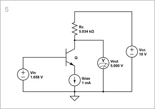
Common-emitter stage with grounded emitter and current output: A BJ transistor has a voltage input (base-emitter junction) and a current output (collector-emitter junction). The simplest way to drive it is to ground the emitter (Ve = 0 V) and apply the input voltage Vin to the base. Figuratively speaking, the emitter is "immovable" and we "move" the base.
simulate this circuit – Schematic created using CircuitLab
In the CircuitLab simulation, open Vin's parameters window and, looking at the ammeter Iout, carefully set the input voltage (658 mV in the schematic) so that a (quiescent) current of 1 mA flows through the collector. This initial input voltage is known as a "bias voltage". You can then wiggle Vin around that value and watch Iout wiggle too around 1 mA.
Common-emitter stage with grounded emitter and voltage output: But our devices "prefer" to work with voltage. So let's insert a resistor Rc in the collector circuit to convert the collector current Iout into an output voltage VRc = Iout.Rc. For convenience, let's use the complementary (to Vcc) voltage Vout which is relative to ground.
simulate this circuit
Now adjust the resistance Rc so that the initial (quiescent) output voltage is equal to half of the supply voltage (5 kΩ in the schematic). Wiggle Vin and watch Vout; the circuit has maximum gain.
Common-emitter stage with "lifted" emitter: The circuit will behave exactly the same (have maximum gain) if we "shift" the emitter and base voltages by, say, 1 V.
simulate this circuit
Conclusion: A transistor stage with a voltage source in the emitter (fixed emitter voltage) has maximum gain because the entire input voltage is applied to the base-emitter junction.
"Soft" emitter
Common-emitter stage with a resistor in the emitter: If when, figuratively speaking, we "move" the base, the emitter also "moves" (in the same direction but with a smaller amplitude), the input voltage applied to the base-emitter junction and, accordingly, the gain decreases... as they say, because of the negative feedback aka "emitter degeneration". We can make the transistor do this by itself if we insert a resistor Re into the emitter (in place of the voltage source).
simulate this circuit
"Very soft" emitter
Common-emitter stage with a current source in the emitter: We can greatly enhance this effect almost zeroing the gain if instead of a resistor we include a current source Ibias or, more precisely, a current-stabilizing non-linear (dynamic) resistor. As a result, the emitter voltage will follow the input voltage exactly and the difference applied to the base-emitter junction will be zero.
simulate this circuit
"Hardened soft" emitter
So these are the rules:
- If we want the transistor stage to amplify as much as possible, we must include a voltage source in the emitter.
- If we want it not to amplify, we must include a current source.
Voltage source in parallel to the current source: We can do this switching easily by connecting the voltage source in parallel without disconnecting the current source; the voltage source overrides the current source. As you can see, this schematic is equivalent to the third schematic above.
simulate this circuit
Variable "softness"
And how do we do the opposite - disconnect the voltage source? Well, here is the biggest trick... The transistor is actually a voltage source (follower) and we have included a second voltage source in parallel which above was causing conflict and high gain. But what if we keep this voltage equal to the emitter (input) voltage? No current will flow between them as if there is no second source. The name of this technique is "bootstrapping".
To implement this idea, we can connect a second emitter follower Q2 in parallel to Q1 and drive its input by an equal input voltage Vin2 = Vin1. As they say, this is the so-called "common mode" input signal.
simulate this circuit
As a result, in the common mode, both base and emitter voltages will change equally and there will be no gain. If we stop the voltage from changing or start changing it opposite to the first voltage (differential mode), the gain becomes maximum.
Now it remains only to draw the schematic more beautifully to get the classic "long-tailed pair".
simulate this circuit
Interacting voltage sources
But now we notice something even more interesting - the Q2's emitter is not only an output (of an emitter follower) but also an input (of a common-base stage). This is because the base-emitter voltage can be varied by both Vb and Ve (the so-called common-base stage). The same goes for Q1. So this is a symmetrical configuration where the two transistors interact (the OP's "interference").
Helping voltage sources (differential mode): When both input voltages change in the same direction, the common emitter voltage follows them, and the two interacting voltage sources "help" each other. Both base-emitter voltages and collector currents do not change; the output voltage also does not change, and the gain is zero.
Opposing voltage sources (common mode): When both input voltages change in the opposite direction, the emitter voltage does not change ("virtual ground"). The base-emitter voltages change with the maximum input voltage amplitude, collector currents change and the gain is maximum. Figuratively speaking, a kind of "tug of war" is observed where one transistor "pulls up" the emitters and the other "relaxes the pull" (at the same time the current source "pulls down" the emitters). Two "pull-up" elements (transistors) and one "pull-down" element (current source) are connected to the common point of the emitters.
Movable ground
I will take advantage of the OP's mistake of connecting the emitters to ground (the second schematic in the body of the question) to show the genius schematic idea here (by the way, when I was doing my thesis in 1980, I also wondered why the emitters were not connected through separate resistors to ground but through a common one).
Long-tailed pair. The clever trick here is that the emitters are connected to a movable but not static ground. Thus, when common-mode (same) input voltages are applied, the ground "moves" with them, and they are not amplified. When differential (opposite) input voltages are applied, the ground does not "move" with them, and their difference is amplified.
OP's pair. In contrast, the OP's transistor emitters are permanently connected to ground. As a result, they amplify equally both common and differential input voltages... but the main requirement of a differential amplifier is to amplify only differential signals and suppress common-mode signals.
Why emitter current source?
This is the second main point in this circuit that remains to be fully clarified. The problem is that the circuit has a differential input but we want its output to be "single-ended" (with respect to ground). A simple ohmic resistor with as much resistance as possible connected between the emitter and ground (or negative power supply) has somewhat solved the problem in the past (and in the H&H bestseller). But when the common input voltages and, accordingly, the emitter voltage Ve vary, the emitter current Ie varies accordingly to Ohm's law - Ie = Ve/Re. So the collector currents and the output voltage vary as well. The problem is because the emitter resistor is constant. If it was a "dynamic resistor" whose resistance increases when the voltage inreases and v.v., their ratio Ve/Re (the current) would stay constant. Accordingly, Ic and Vout would not change.
So, the common device between the emitters and ground (the circle with an arrow inside) is not a true current source (producing a current) but a constant-current dynamic resistor (setting the current). It is usually implemented by another transistor with a constant input voltage.
Limitations
Maximum common-mode voltage: Due to the significant gain, the input differential voltage is insignificant against the background of the common-mode voltage, which varies widely; let's see in what limits.
When both input voltages simultaneously increase (common mode), the emitter current "source" increases its internal resistance with the same rate. In the same time, the collector-emitter jubctions decrease their "resistance" with the same rate. As a result, the total resistance between the supply rails, quescient collector current and output voltage do not change. Only there is a "small"problem.
The voltage drops across the collector-emitter junctions continuosly decrease and when approach zero, transistors exhaust their supply of "resistance" and as they say, they saturate. So, the common-mode voltage is limited above by the quiescent collector voltage.


