6

I have a board with an Altera EPF10K30RC240-4N that is not functioning at all. There is a high current draw on the board. The +5V rail is only 2.6V and there is 4.2 ohms between +5V and GND.

The board is a plug-in module for a larger assembly. It has been operating without fault for over 20 years, so no, the chip is not installed incorrectly. When a known good board is installed, the system works perfectly; it is not the power supply. Nor is it the clock or the program, that would not explain the 4.2 ohms to ground.

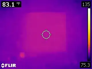
Looking at the board with a thermal camera, the FPGA is the only device that is heating up abnormally. The entire chip gets warm within seconds. Comparing the thermal image to the working board, it should only be a few degrees above ambient temperature when running.

The question is: what would cause an entire FPGA package to heat up evenly across the whole device? If there was a shorted gate or I/O driver, I would expect to see a heat bloom at that specific spot on the die.

FPGA heating up over 52 seconds (low-res 320x240 camera):

enter image description here

enter image description here

ADDENDUM 08/31/23

I removed the chip and discovered a blow-out on the bottom side. After removal, the resistance between the +5V and GND rails on the board went to 3.9k. So the chip is shorted internally and is dead, as was mentioned in the two answers below. (Excuse the bent pins, I clumsily dropped the chip immediately upon removal {roll eyes}).
enter image description here

colintd
  • 2,018
  • 2
  • 17
jfriend
  • 465
  • 1
  • 10
  • 1
    When is the 4.2 ohms measured -- unpowered? Or at voltage (so load current is a hair under half an amp)? Do any IOs measure +V, GND or indeterminate? FWIW, the chip is pretty small (<= 1cm?), hidden under the heat spreader; I would be surprised if more than a general (chip-sized) hotspot were resolvable. – Tim Williams Aug 31 '23 at 13:59
  • 1
    The 4.2 ohms is measured with the board out of the mainframe. Some I/Os are 0V and a few others are +V (although only a few volts as the entire +5V is low). – jfriend Aug 31 '23 at 14:41
  • 2
    Perhaps caused by latch-up within the substrate. Often hard to track down. – glen_geek Aug 31 '23 at 14:45
  • This may just be a trick of the perspective, but is the bottom row of pins aligned with the pads? – 1N4007 Aug 31 '23 at 16:28
  • Is it just one board in this state? Are there many other boards working fine? – colintd Aug 31 '23 at 16:31
  • 1
    @1N4007: It is perspective. The pins are misaligned less than 1/4 the width of the pads. And the space between the pads is greater than their width. – jfriend Aug 31 '23 at 16:32
  • Yes, it is just this one board. There are other boards in the mainframe (not the same board, not the same chip) and everything else is working. I have several more of these mainframes and they all work perfect. – jfriend Aug 31 '23 at 16:34
  • Any luck repairing the board with a new FGPA? – colintd Sep 01 '23 at 08:52
  • 1
    The replacement chip is ordered, it will be a few weeks before we'll know. I will follow up on this thread at that time. – jfriend Sep 01 '23 at 22:06

2 Answers2

7

From memory, this family of devices has the die mounted directly to the underside of the large copper heat spreader, which is visible as the silver area in the middle of the chip.

The conductivity is such that even heat from a point sources on the die, very quickly spreads out (hence the name), and given the relatively slow rate of heating, I would absolutely not expect to see any localized heat signature from the top of the heat spreader.

You might try looking at the underside of the PCB, because this might show more localized heating (even on the opposite side of the PCB).

I would therefore guess that this device has suffered some kind of catastrophic failure, effectively shorting the supply rails internally. This TI paper on latch up is worth reading, because if the condition exists for an extended period of time, it can cause permanent damage.

If you want to track further, then I would look at the voltage gradient (relative to source ground, with mV precision) across the various power vias on the PCB and supply pins to the device. I suspect you will find one set of power pins to the device shows the lowest delta anywhere on the PCB, confirming the fault is inside the device (thought it might also indicate the problem is elsewhere).

If you were brave, you could carefully lift all the power pins, and verify whether the short disappears. Probably very little to lose, as the chip is almost certainly dead.

colintd
  • 2,018
  • 2
  • 17
  • 2
    I removed the chip and found a blowout on the bottom. It is definitely shorted. Board +5V rail resistance went up to 3.9k after removal. – jfriend Aug 31 '23 at 21:43
  • 1
    Once the "magic smoke" comes out all bets are off! – colintd Aug 31 '23 at 22:14
  • The kind of damage shown in the photo is very indicative of a point fault (latch up or I/O gate punch through due to ESD) which persisted for long enough to cause permanent failure. – colintd Aug 31 '23 at 22:18
  • 1
    Thanks for reporting back, and marking as an answer. It makes the question much more useful to others. – colintd Aug 31 '23 at 23:09
2

what would cause an entire FPGA package to heat up evenly across the whole device? If there was a shorted gate or I/O driver, I would expect to see a heat bloom at that specific spot on the die.

I agree. If indeed a small part of the die was causing the short, and you were looking at the die itself, that’s what you’d see - minus the effects of lateral heat conduction through he die acting to smear the heat signature somewhat.

Alas, the idea that the failure is localized is not necessarily sound. Failures of certain kind propagate, and it a failure results in significant substrate current gradients, it may latch up the entire chip instantly. Or it may not. Hard to say. But it’s not at all a given that a small localized failure won’t cause the whole chip to misbehave. A failure could cause common lines to be driven by multiple sources, just as a simple “non-exotic” example.

And also: you’re talking about the die, but not looking at the die, but at a packaged chip, and more specifically at a large chunk of metal in the chip’s package. The chip’s thermal design would have to be done very poorly to see any detail in the thermal image. A good part of the job of the packaging engineer was to maintain the die at an even temperate and with good contact with outside.

Is the chip dead? Yes.

Now, if you didn’t have a thermal imaging camera, you might have used higher temperature resolution methods of measurement, and then it’s likely you’d see a bit of a gradient from one edge or corner of the heat spreader to the other. The resolution needed for that is on the order of 1mK, so quite beyond what a consumer thermal camera can do. It’s not likely you’d see a clear peak inside the heat spreader though.