The textbook stage, as shown, is a high-gain (AC) amplifier that generates highly distorted outputs. Alone, without a global NFB network, it's rarely used. This is because the AC voltage gain depends upon \$r_e^{\:'}\$ working against \$R_{_\text{L}}\$ and for good or bad it's a fact that \$r_e^{\:'}\$ depends upon the instantaneous value of \$I_{_\text{E}}\$, itself varying with the input signal (as it must do.) When the AC voltage gain depends upon the instantaneous value of the input signal, the result is distortion. This stage should not be used without the application of negative feedback to manage the AC gain better.
So there is already a problem. And that problem adds to your question.
You also mention class-A.
Luckily, all can be directly addressed in a single, simple solution.
Something like this:
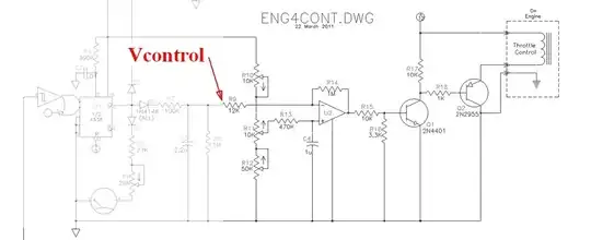
simulate this circuit – Schematic created using CircuitLab
(The above circuit can be arranged in either BJT polarity, of course. I chose one. But the opposite could equally be chosen, as well.)
The current sink can be formed using two BJTs. I recommend reading jonk's writing here for details. For the above diagram, I assume you can follow those instructions to replace behavioral \$I_1\$ with a practical subcircuit.
The open loop voltage gain will be very high since \$Q_2\$ will be working against a very stiff current sink. The closed loop voltage gain is set using \$R_{_\text{Y}}\$ and \$R_{_\text{Z}}\$ and should be slightly less than \$1+\frac{R_{_\text{Y}}}{R_{_\text{Z}}}\$. (All the capacitors, including \$C_{_\text{Z}}\$, need to be large enough, but their accuracy probably isn't critical.)
The DC biasing needs to take some details into account. But it's not hard to do.
I think this directly addresses your questions about how to modify the circuit, use class-A, and get both voltage and current gain at the output. And you can readily set the output current compliance using \$I_1\$'s set value. (I chose \$3\:\text{mA}\$ only as an example to consider. Not a requirement, of course.)
The important thing to note about here is that the schematic provides global NFB. This is vital to a managed design. It also provides for a very high input impedance, as \$Q_1\$'s base current is rather low (when the output compliance is expressed in small milliamps, then the base current is expressed in just tens of nanoamps.) This topology is an important one to learn about! I can't express it in words with enough emphasis!
If you come up with a specific set of specifications, I'd be happy to work out specific values for the above schematic.
As a final note, there are several ways to arrange biasing the base of \$Q_1\$. I've shown just one option. There are others and, as it turns out, what you chose depends somewhat on your power supply rail details (voltage, range of voltage over time of use -- if a battery, ripple, noise, etc.) But the basic behavioral idea is there in the schematic above.
