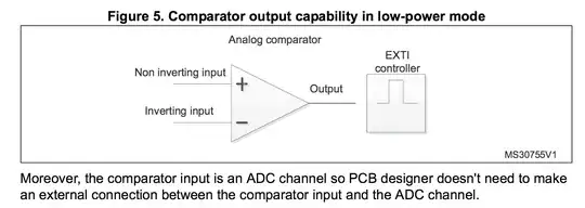
If the voltage at the capacitor exceeds a level Vdc,max the comparator should output high, if the voltage falls below the level Vdc,min the comparator should output low.
The comparator with hysteresis may not be a solution to your problem. Because with hysteresis, the max and min points change slightly around the original reference point (the reference without the hysteresis).
So window comparator might be what you need:
If the comparator with hysteresis what you need, here's your answer:
is this the right approach?
I couldn't understand your approach but here's how I calculate:
Without the extra resistor (from output to non-inverting input) the trigger point would be the reference voltage (voltage at the inverting input). Quite simple:
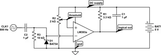
simulate this circuit – Schematic created using CircuitLab
With the extra resistor the division ratios will change. Assume the comparator gave an output of HI (VCC):

simulate this circuit
So if you calculate Vtrig_HI from the divider network above that'll be the max trigger point.
Likewise, assume the comparator gave an output of LO (GND):
simulate this circuit
Again, if you calculate Vtrig_LO from the divider network above that'll give you the min trigger point.
EXAMPLE:
VX = 10V, R1 = 10k, R2 = 1k, and comparator's supply is VCC = 5V.
Without any hysteresis the trigger point would be 2V.
But if we add an extra resistance of R3 = 20k for hysteresis, using the two diagrams above, the low trigger would be 1.92V and the high trigger would be 2.11V.
simulate this circuit
For HI, solve the following for Vtrig-HI:
$$
\mathrm{
\frac{10V-V_{trig-HI}}{4k}+\frac{5V-V_{trig-HI}}{20k}=\frac{V_{trig-HI}}{1k}
}
$$
And for LO, solve the following for Vtrig-LO:
$$
\mathrm{
V_{trig-LO} = 10V \cdot \frac{(1k \ || \ 20k)}{4k+(1k \ || \ 20k)}
}
$$
You can derive the equations if you want. During a design, I normally put the calculations into an Excel file and play with the values (cells) to see how trigger points change.


