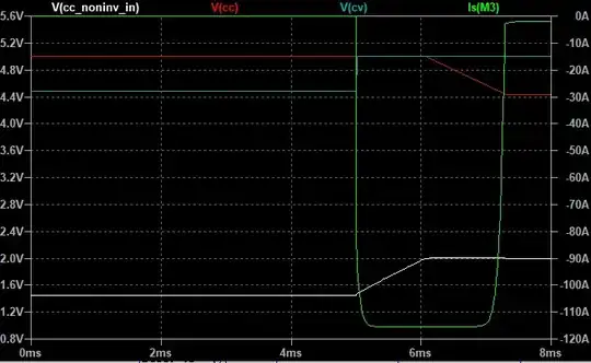
I want to design a linear regulator based on NMOS with CC/CV capability. I made a circuit with two separate loops (CC and CV), each of which is stable. The problem is in the transition moment when the circuit is under light load and the CV loop is regulating the output. When I shorten the output, the current through mosfet is almost unlimited until the CC loop kicks in. But this transition is really slow. What would be a better design of the CC/CV loop in this case?


Asked
Active
Viewed 47 times
3
Vasiliy
- 85
- 3
-
How big of a swing does the output of say the CV loop opamp need to take when it kicks in? How fast does it come out of saturation? – winny Aug 23 '23 at 21:44
1 Answers
1
Both CC and CV controls have the same level of priority; look at the two transistors that arbitrates (Q2 versus Q4). This is bound to end in tears. The shared collector node also doesn't have a pull-down resistor and this will help speed responses up.
Please also add a 1 kΩ resistor in series with Q1's collector.
You might find that adding a resistor in series with Q2's collector helps reduce the priority issue mentioned above. Also add a 1 kΩ resistor in series with Q1's base. There may be other issues but, these stick out like a sore thumb.
Andy aka
- 434,556
- 28
- 351
- 777
-
This; an emitter resistor on Q1, Q2 and Q4 to set transconductance would also be quite welcome for stability. – Tim Williams Aug 23 '23 at 20:53
-
Since current has already been limited by R2 (300Ω), why do we need a 1 kΩ resistor in series with Q1's collector? 1 kΩ won't allow the gate to go to a low voltage when the output should be low. – Vasiliy Aug 23 '23 at 21:09
-
1Current hasn't been limited by R3 when the MOSFET M3 is close to full conduction. Current (plenty) will flow through D1 and D2 and damage Q1. Also, the added resistor reduces loop gain (a possible benefit). – Andy aka Aug 23 '23 at 22:05
