0

I'm writing an emulator for the MOS 6502 processor.
In order to test it, I decided to run the ROM from the Apple 1.

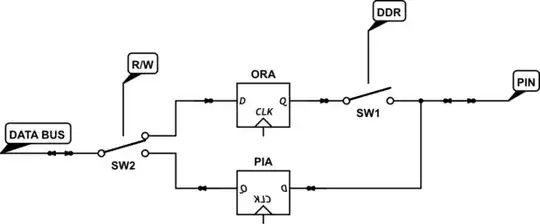
The Apple 1 uses a Motorola MC6820 PIA (Peripheral Interface Adapter) for communication between the CPU and the keyboard/display.

I'm trying to emulate the MC6820 so I can have keyboard support, but I'm having trouble understanding how it is supposed to work.

Memory is mapped the following way:

0xD010: Keyboard Data
0xD011: Keyboard Control Register
0xD012: Display Data
0xD013: Display Control Register

The ROM does the following, with original comments:

            LDY #$7F     ; Mask for DSP data direction register.
            STY $D012    ; Set it up.
            LDA #$A7     ; KBD and DSP control register mask.
            STA $D011    ; Enable interrupts, set CA1, CB1, for
            STA $D013    ;  positive edge sense/output mode.
            ...          ; Other initialization code...
NEXTCHAR    LDA $D011    ; Key ready?
            BPL NEXTCHAR ; Loop until ready.

At reset, all bits on the PIA will be 0.
As bit 3 (DDR) of the control registers are 0, a data write will end up in the corresponding data direction register.
So:

LDY #$7F
STY $D012

Will write 0x7F into the data direction register B, configuring bits 0-6 as outputs.
This is for the display.

Then the value 0xA7 is written to control registers A and B:

LDA #$A7
STA $D011
STA $D013

I'm already having trouble understanding this.
Based on the documentation, bits of the control registers are:

| 7    | 6    | 5, 4, 3    | 2   | 1, 0       |
| IRQ1 | IRQ2 | C2 Control | DDR | C1 Control |
| 1    | 0    | 1  0  0    | 1   | 1  1       | => `0xA7`

DDR bit is set to 1, so data read/write will end up in the output register A or B and no longer in the data direction register A or B.

But why the other flags?
And what happens on the PIA at this exact time?

When the ROM checks for a key press:

LDA $D011    ; Key ready?
BPL NEXTCHAR ; Loop until ready.

It checks if bit 7 of the control register is set, meaning it shouldn't be set until a key is pressed.

But it has initially be set to 1 with the value 0xA7.
So how was it reset?

Does setting 0xA7 generate an interrupt, making the CPU read the value, as, as I understand, a read by the CPU should clear the IRQ flags?

Macmade
  • 281
  • 6
  • 16

1 Answers1

3

Refer to MC6821 datasheet. Read this carefully, over and over. I went through several misunderstandings before getting it right.

DDR bit is set to 1, so data read/write will end up in the output register A or B and no longer in the data direction register A or B.

Write data will end up in the output register. Peripheral input data is routed directly to the data bus.

But why the other flags?

Only bits 6 and 7 are flags. They are read-only. The rest are read write. Writing to 6 and 7 has no effect.

The value 0XA7 is a mask that is used to extract bits of interest to the program from a read of the control register. It doubles as the actual value of the bits needed to configure the control register. Since the MSB cannot write to its position, it is ignored on a write. Just a convenience for the programmer.

There is no activity internal to the PIA that will cause interrupts. They can be controlled by CRA/B bits [1,0] according to Table 3.

enter image description here

This allows input activity on CA1/CB1 to pass an interrupt signal to the MPU or not.

It checks if bit 7 of the control register is set, meaning it shouldn't be set until a key is pressed

In the OP's example, when any key is pressed, an interrupt is asserted on CA1/CB1 (according to 0xA7 control register mask). This will set the corresponding IRQ7 flag in CRA/CRB.

Does setting 0xA7 generate an interrupt, making the CPU read the value,

LDA $D011 ; Key ready?
BPL NEXTCHAR ; Loop until ready.

It looks like it is not using an MPU interrupt, but polling the flag until it goes high.

But it has initially be set to 1 with the value 0xA7. So how was it reset?

As discussed, bit 7 cannot be written. It can be set only by activity on CA1 (keypress). It is cleared (reset) by a read of the associated data register.


CA2/CB2 can be set as outputs if Bit 5 is high. The other two bits set the behaviour. CA2 behaves differently from CA1. These pins are available to the keyboard and display. The state of the output can change depending on the activity on CA1/CB1 as well as activity from the MPU.

Tables 5 and 6 show how CA2/CB2 can be used as outputs. It is not easy to understand why the implementation is as described. These outputs to the peripheral can be used as on-off, LED switches etc.

For the MCU to turn an LED on and off, CRA/CRB bit three can be written to force CA2/CB2 high or low.


Addition from comment

The ORA/ORB cannot be read directly. Only the PIA/PIB can be read. An ORA bit can be read only if the DDR connects it to a PIA line.It is always connected to the peripheral lines, whether they are input or output pins. The DDR just connects the ORA to the specified PIA line. If all the PIA lines are inputs, then the ORA cannot be read. Motorola does not make clear how this is done but I speculate something like as in the schematic:

schematic

simulate this circuit – Schematic created using CircuitLab

RussellH
  • 12,496
  • 2
  • 9
  • 34
  • Thanks a lot for the detailed answer. I think I'm beginning to understand. So by writing `0xA7` to `CRA`, only `0x27` will be effectively written, as bits 7 and 7 are read-only. By setting bits 0 and 1, it enables IRQs so the next time a key is pressed, bit 7 will be set on `CRA`. The loop will then read `CRA`. As bit 7 is now set by a keypress, it will then read `ORA`, which will reset bit 7 of `CRA` to zero. Is this right? – Macmade Aug 22 '23 at 09:20
  • Yes that is correct. Except the ORA cannot be read directly. See my addition to my answer.@Macmade – RussellH Aug 22 '23 at 15:18
  • Thanks a lot! Great answer! – Macmade Aug 22 '23 at 15:37